I'm working on a simple power amp output stage. My main design goals are:
* very low output impedance (will be driving a 2ohm speaker)
* rail-to-rail voltage swing
I'd like to operate this amp with a single rail 12V power supply, so I can't afford to lose 0.6V all over the place, which most BJT followers do.
I think a MOSFET based design is the way to go, but correct me if i'm wrong.
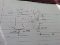
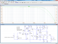
This is the design i've come up with (the first picture); it uses 2 IRF540 MOSFETs in a quasi-complementary topology fed by a differential pair. The top mosfet has its own separate positive supply rail supplied by a capacitor that is charged whenever the output is low. That supply rail is kept at an almost constant voltage above the mosfet's source. This allows the gate voltage to go above the main supply rail, and allows the output to reach +6V.
The 2n7000 acts as a current buffer; it is there in order to keep Vce of the input BJTs constant and thus avoiding the early effect.
There are a number of problems with this design; the biggest one is that the point at the base of the topmost 2n3906 exhibits negative resistance behavior; if you draw current out of it, it will respond by raising its own voltage. In my prototype circuit this sometimes causes oscillations. The issue was worked around by adding an RC circuit around the capacitor, limiting dv/dt at the secondary supply rail.
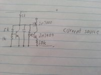
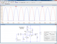
The second picture is the current source circuit i'm using (for supplying the differential pair).
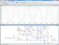
I've currently tested with 100% negative feedback (output shorted to the "-" input), and I don't hear any harmonic distortion (played back a 35Hz sine wave and listened to it). I don't have any equipment that can allow me to measure the THD, but it doesn't really matter for now as this is a pet project not meant for very high quality audio. As long as I can't hear distortion (both when playing a sine wave and music), it's good enough.
The resistor values I'm testing with are:
* 20k at the 2n3906s
* 5k at the mosfets
I might run this amplifier with slightly higher voltages, but usually nothing higher than 24V (-12V and +12V).
Looking around the forum (and on the internet), I've never seen a design like this; is there a reason people don't use op-amp style output stages? in my case op-amp style is necessary because I need a gain >1; otherwise pre-amp stages before this will also need rail-to-rail swing in order to get rail-to-rail swing at the final output.
I'd like some feedback (no pun intended) on my design; is there something fundamentally wrong with the way I'm designing my output stages? which other designs would you recommend and why? what about BJT based designs? is near rail-to-rail voltage swing practically achievable with those?
* very low output impedance (will be driving a 2ohm speaker)
* rail-to-rail voltage swing
I'd like to operate this amp with a single rail 12V power supply, so I can't afford to lose 0.6V all over the place, which most BJT followers do.
I think a MOSFET based design is the way to go, but correct me if i'm wrong.
This is the design i've come up with (the first picture); it uses 2 IRF540 MOSFETs in a quasi-complementary topology fed by a differential pair. The top mosfet has its own separate positive supply rail supplied by a capacitor that is charged whenever the output is low. That supply rail is kept at an almost constant voltage above the mosfet's source. This allows the gate voltage to go above the main supply rail, and allows the output to reach +6V.
The 2n7000 acts as a current buffer; it is there in order to keep Vce of the input BJTs constant and thus avoiding the early effect.
There are a number of problems with this design; the biggest one is that the point at the base of the topmost 2n3906 exhibits negative resistance behavior; if you draw current out of it, it will respond by raising its own voltage. In my prototype circuit this sometimes causes oscillations. The issue was worked around by adding an RC circuit around the capacitor, limiting dv/dt at the secondary supply rail.
The second picture is the current source circuit i'm using (for supplying the differential pair).
I've currently tested with 100% negative feedback (output shorted to the "-" input), and I don't hear any harmonic distortion (played back a 35Hz sine wave and listened to it). I don't have any equipment that can allow me to measure the THD, but it doesn't really matter for now as this is a pet project not meant for very high quality audio. As long as I can't hear distortion (both when playing a sine wave and music), it's good enough.
The resistor values I'm testing with are:
* 20k at the 2n3906s
* 5k at the mosfets
I might run this amplifier with slightly higher voltages, but usually nothing higher than 24V (-12V and +12V).
Looking around the forum (and on the internet), I've never seen a design like this; is there a reason people don't use op-amp style output stages? in my case op-amp style is necessary because I need a gain >1; otherwise pre-amp stages before this will also need rail-to-rail swing in order to get rail-to-rail swing at the final output.
I'd like some feedback (no pun intended) on my design; is there something fundamentally wrong with the way I'm designing my output stages? which other designs would you recommend and why? what about BJT based designs? is near rail-to-rail voltage swing practically achievable with those?
Attachments
Have a look at the CIRCLOMOSLooking around the forum (and on the internet), I've never seen a design like this;
Have a look at the CIRCLOMOS
I looked at your circuit; correct me if i'm wrong, but it seems that the mosfet driver circuit is such that Vgs{M1} + Vgs{M2} is constant:
R9 supplies a constant current which is split into two paths: R1 and R2; this means that I{R1}+ I{R2} = constant, which means V{R1} + V{R2} = constant; Vgs{M1} is simply V{R1} plus the zener voltage, 4.7V.
What this implies is that the maximum Vgs that could be supplied to a mosfet is 2 times the idle Vgs. At a Vgs(th) of about 3V, the max Vgs is 6V, which may not be enough to turn the mosfet completely on. Now it seems that Q1 might be able to pull R9 down lower, increasing the current and Vgs of M2, but M1 is still restricted to twice Vgs(idle). This could cause asymmetrical saturation characteristics. This might not be an issue if your idle current is set really high though.
The voltage shifter in your circuit is pretty clever but unfortunately it's not quite enough for my applications: when the output is at +Vcc, there is only enough voltage in C3 to barely turn on M1. In my case I can't afford to lose even 0.5V.
I also prefer low quiescent currents; usually no more than 20mA.
I ended up going with a charge pump to get a low-current +22V rail and got rid of the negative resistance part; I'm using a simple 4-transistor charge pump circuit (capacitor based); I've also ordered P-channel mosfets (IRF9540) and will investigate using a complementary design instead.
Background: the application is a simple low-power efficient amplifier for casual music listening. I only have 12V power supplies (PC power supplies) and there are no electronics parts stores where I live where I can get a reasonably-priced switched mode power supply. I have relatives in china who visits often and can bring parts, but I wouldn't trust power supplies from china 😀
You are right in your analyzis, and with lat-fets, the constant-sum mechanism would severely limit the output capabilities.I looked at your circuit; correct me if i'm wrong, but it seems that the mosfet driver circuit is such that Vgs{M1} + Vgs{M2} is constant:
R9 supplies a constant current which is split into two paths: R1 and R2; this means that I{R1}+ I{R2} = constant, which means V{R1} + V{R2} = constant; Vgs{M1} is simply V{R1} plus the zener voltage, 4.7V.
What this implies is that the maximum Vgs that could be supplied to a mosfet is 2 times the idle Vgs. At a Vgs(th) of about 3V, the max Vgs is 6V, which may not be enough to turn the mosfet completely on. Now it seems that Q1 might be able to pull R9 down lower, increasing the current and Vgs of M2, but M1 is still restricted to twice Vgs(idle). This could cause asymmetrical saturation characteristics. This might not be an issue if your idle current is set really high though.
With modern V-Dmos, the characteristic is a very steep exponential and it poses no particular problem unless you want to drive really low loads with a low initial Iq.
The constant-sum provides an excellent complementarity, better in fact than actual N/P complements, which is why I favored it.
I have also used it in the Circlophone, where the constant sum is a non issue because of the BJT OP's
Some car-radio amplifiers are quite efficient in this respect, they use common emitter or source OP, and they swing to within a few hundred mV of either rail.Background: the application is a simple low-power efficient amplifier for casual music listening. I only have 12V power supplies (PC power supplies) and there are no electronics parts stores where I live where I can get a reasonably-priced switched mode power supply. I have relatives in china who visits often and can bring parts, but I wouldn't trust power supplies from china 😀
Note that other routes are possible:
http://www.diyaudio.com/forums/solid-state/246323-new-toy-play-symclophone.html
http://www.diyaudio.com/forums/solid-state/246642-synclophone.html
http://www.diyaudio.com/forums/soli...-mini-transistor-amplifier-5.html#post2904409
http://www.diyaudio.com/forums/soli...-mini-transistor-amplifier-5.html#post2904596
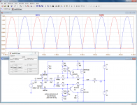
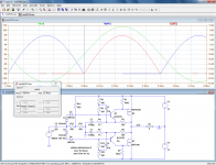
So I took some ideas from your designs and came up with this complementary design (image attached). The Vgs(max) = 2Vgs(idle) issue came up in this design. With a 2 ohm load the THD shoots up to 1.8%, and clipping is visible in the output waveform (clips at 1V). Idle current is 20mA.
My question is: what kind of mosfets are usually lateral and which ones vertical? The datasheet usually doesn't say; In the simulation I'm using IRFP240/9240 because there aren't models for the IRF540/9540. Will there be a noticeable difference with the IRF540/9540? The datasheet says 10A@Vgs=4.5V for IRF540 vs 5A@Vgs=4.5V for the IRFP240.
I haven't prototyped it yet as I'm still waiting for my P-mosfets to arrive.
What do you think of the circuit topology in general? any modifications you'd suggest? I'm fairly new to audio amplifier design (although i've designed and built a crappy amplifier back in grade 9 which I've used for 5 years and am now wanting to replace with a better design).
Attachments
All the cheap, commonly available types are V-fets, including the IRF series.My question is: what kind of mosfets are usually lateral and which ones vertical? The datasheet usually doesn't say;
This series is quite old, though and the transconductance is minuscule compared to modern types: with these types, the characteristic is so steep that it rivals Bjt's. They would solve neatly your 2*Vg issues
The 240 are larger, but they are higher voltage, meaning higher ressistivityIn the simulation I'm using IRFP240/9240 because there aren't models for the IRF540/9540. Will there be a noticeable difference with the IRF540/9540? The datasheet says 10A@Vgs=4.5V for IRF540 vs 5A@Vgs=4.5V for the IRFP240.
I haven't prototyped it yet as I'm still waiting for my P-mosfets to arrive.
It looks promising, but in practice you'll also have to include provision for device to device variation and quiescent current controlWhat do you think of the circuit topology in general? any modifications you'd suggest? I'm fairly new to audio amplifier design (although i've designed and built a crappy amplifier back in grade 9 which I've used for 5 years and am now wanting to replace with a better design).
Last edited:
After some thought I came up with this N-only design; it is very similar to the circlomos, but with easier biasing. The bias current can be adjusted without disturbing the dc balance at the input stage.
The differential stage is fed with the same amount of current as the output "default" current, with the result that when the input is balanced, half of the default current is diverted to the lower mosfet, and the output is also balanced.
This scheme has less open-loop gain, so I added a second differential stage to boost the gain.
In spice, clipping occurs at 11.5V and 0.5V with a 2-ohm load. I'm using IRF540N in the actual build so hopefully it'll be better.
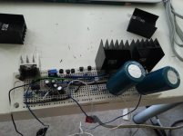
I've built the circuit on a breadboard and it works well enough. I can't hear any harmonic distortion other than the distortion caused by one of the speakers. (I'm using 2 4-ohm speakers in parallel, and one of them makes a small distortion sound when playing a sine wave)
I used a simple 4-transistor charge pump to provide the 20V rail, and used an output capacitor because I don't have a split-rail power supply.
R4 and R6 are replaced with a trimmer to adjust the bias current.
If R13 and R14 are reduced to 100 ohm, in spice I can get a THD of about 0.015% (with the same amount of feedback as shown in the attached picture). However the circuit becomes unstable in the actual build, making a harsh sound whenever clipping occurs. I suspect there is high frequency oscillation that is normally not sustainable but is triggered during clipping.
The differential stage is fed with the same amount of current as the output "default" current, with the result that when the input is balanced, half of the default current is diverted to the lower mosfet, and the output is also balanced.
This scheme has less open-loop gain, so I added a second differential stage to boost the gain.
In spice, clipping occurs at 11.5V and 0.5V with a 2-ohm load. I'm using IRF540N in the actual build so hopefully it'll be better.
I've built the circuit on a breadboard and it works well enough. I can't hear any harmonic distortion other than the distortion caused by one of the speakers. (I'm using 2 4-ohm speakers in parallel, and one of them makes a small distortion sound when playing a sine wave)
I used a simple 4-transistor charge pump to provide the 20V rail, and used an output capacitor because I don't have a split-rail power supply.
R4 and R6 are replaced with a trimmer to adjust the bias current.
If R13 and R14 are reduced to 100 ohm, in spice I can get a THD of about 0.015% (with the same amount of feedback as shown in the attached picture). However the circuit becomes unstable in the actual build, making a harsh sound whenever clipping occurs. I suspect there is high frequency oscillation that is normally not sustainable but is triggered during clipping.
Attachments
I do not know about the specific parameters in your simulator, but real mosfets, especially the high Gm vertical ones must have some sort of local frequency compensation. Most of the time a gate stopper resistor is used. In addition to the gate stopper, I like to also include a gate to drain Zobel (that is, a small zero placed from gate to drain ~30MHz). If you take apart a mosfet and look at the 'internal components' you will find they tend to make great RF oscillators and must be damped accordingly. At audio frequencies the tiny inductance of the wire (and component lead/bonding wires to die) has a negligent effect. At RF the story is different. The gate stopper is important here. If you look at the datasheet you will notice in the capacitance graph that as Vds approaches saturation (clipping) the input capacitance increases significantly......specifically Cgd. This makes the mosfet more likely to burst into oscillation at the output peaks where Vds is minimum. Nothing can be done about that other than either don't drive the device to Vds saturation which is impractical or add the proper compensation. The gate stopper resistor and gate to drain Zobel should be as close to the device package as possible, minimizing lead length and lead inductance. Although you are building an audio frequency amplifier, proper RF layout and compensation is certainly necessary when using mosfets.

Last edited:
The arrangement is interesting, but I think it has some weaknesses:After some thought I came up with this N-only design;
R1 and R2 are very large, and this will cause problems under large signal/high frequency conditions, especially with bigger, high-capacitance MOS.
The mirroring by Q6/Q7 is original, but I think its performances will be poor compared to a more conventional circuit: the Hfe matching/tracking between complementary transistors won't be very accurate, and the base node will have a high impedance, making it sensitive to the base capacitances.
Without source resistors, there is a real risk of thermal runaway.
No explicit compensation scheme is included, which is why you run into problems as soon as you increase the loop gain. You should make a proper Bode analyzis, and include deterministic compensation components.
Note that the compensation of two stages will be rather tricky.
I tried that (series RC between gate and drain), and it seemed to make things worse.I like to also include a gate to drain Zobel
I'm generally not a fan of Zobel networks after the output stage because the resistor can easily burn if high frequency signals are somehow present. Using a higher power resistor is not an option because they are very expensive.
As for gate stopper resistors, this is my understanding of it (correct me if i'm wrong):
adding gate stoppers causes low-pass filtering of the signal, and shifts the 0dB gain point to a lower frequency where the phase shift is smaller (and farther from 180 degrees where oscillation would occur). I think using a larger gate-source resistor and a smaller bias current would achieve the same thing.
That is a deliberate design choice; I decided to trade off high frequency performance (>15kHz) for lower idle power consumption. Since the bias current is drawn from the +20V rail which is provided by the inefficient charge pump, it's important to keep the current draw low.The arrangement is interesting, but I think it has some weaknesses:
R1 and R2 are very large, and this will cause problems under large signal/high frequency conditions, especially with bigger, high-capacitance MOS.
The problem with the conventional current mirror is that it is subject to temperature drift (the output transistor heats up more and has lower Vbe). In past experiments I found that just touching one of the transistors causes a non-negligible change in current gain. I also found that in my transistor sample, variations in Hfe are usually much smaller than variations in Vbe, so I generally prefer to use this kind of current mirror. High frequency operation isn't important, so the capacitance is not an issue.The mirroring by Q6/Q7 is original, but I think its performances will be poor compared to a more conventional circuit: the Hfe matching/tracking between complementary transistors won't be very accurate, and the base node will have a high impedance, making it sensitive to the base capacitances.
Thermal runaway is usually not an issue for me because with adequate heat sinking, the temperature has to be pretty high for the power created by Iq (rate at which heat is generated) to be greater than the dissipation rate (rate at which heat is removed). I only care about stability below 50*C (case temperature).Without source resistors, there is a real risk of thermal runaway.
If thermal runaway does occur, the overcurrent circuit will trip long before any damage is done. I always make sure that at the trip current, the power supplied is less than what the heat sink can handle while keeping within the SOA of the output transistors. Even during thermal runaway, power dissipation is usually balanced across the 2 transistors, so supplying 2 times maximum dissipation of each transistor is fine too.
Also, I don't have any resistors available that are less than 10 ohm right now, and it's impossible for me to order anything at this time.
A 1W low-value resistor cost about the same as a IRF540 mosfet in the electronics parts market I buy stuff from (about $0.25 usd).
I tried including a compensation capacitor similar to the way you did in the circlomos, and although it stabilized the circuit in spice, in the actual build it makes little to no difference.No explicit compensation scheme is included, which is why you run into problems as soon as you increase the loop gain. You should make a proper Bode analyzis, and include deterministic compensation components.
Note that the compensation of two stages will be rather tricky.
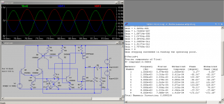
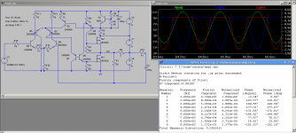
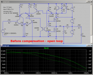
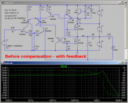
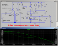
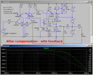
Attached are the before/after transfer functions.
Any idea what the problem is? Am I using the frequency response thing correctly? (I've only been using spice for 5 days).
Anyways, the amp as-is is aleady "good enough" for my uses. With R13 and R14 set to 1K, the circuit is stable enough in real life. There are no thermal issues; the output transistors only warm up slightly when playing music at the loudest volume I'd want to play it here, and doesn't get hot even with a continuous tone. Total idle current is ~60mA (mainly used by the charge pump oscillator).
Attachments
Gate stoppers only prevent local instabilities caused by the high transconductance and parasitics of the layout.As for gate stopper resistors, this is my understanding of it (correct me if i'm wrong):
adding gate stoppers causes low-pass filtering of the signal, and shifts the 0dB gain point to a lower frequency where the phase shift is smaller (and farther from 180 degrees where oscillation would occur). I think using a larger gate-source resistor and a smaller bias current would achieve the same thing.
One tries to avoid an effect on the global stability since they tend to introduce unwanted phase-shifts.
They are a necessary evil, and they should be kept minimal.
In your design, the upper MOS can go away with it, provided your layout is not too lousy.
For the lower MOS with a direct follower drive, it is prudent to include one.
You have more than traded the HF performance, see the squarewave sim below: the amp is not even capable of a full negative swing, and the slew rate is in the region of 0.35V/µsThat is a deliberate design choice; I decided to trade off high frequency performance (>15kHz) for lower idle power consumption. Since the bias current is drawn from the +20V rail which is provided by the inefficient charge pump, it's important to keep the current draw low.
The problem with the conventional current mirror is that it is subject to temperature drift (the output transistor heats up more and has lower Vbe). In past experiments I found that just touching one of the transistors causes a non-negligible change in current gain. I also found that in my transistor sample, variations in Hfe are usually much smaller than variations in Vbe, so I generally prefer to use this kind of current mirror. High frequency operation isn't important, so the capacitance is not an issue.
I tried including a compensation capacitor similar to the way you did in the circlomos, and although it stabilized the circuit in spice, in the actual build it makes little to no difference.
Attached are the before/after transfer functions.
Any idea what the problem is? Am I using the frequency response thing correctly? (I've only been using spice for 5 days).
The bases node is really too sensitive to attach anything without ruining further the dynamic behaviour.
I have simply used more balanced degeneration resistors and a phase advance cap on the FB resistor, it provides >60° phase margin at all frequencies, which is not brilliant, but with two stages the compensation options are limited.
If it is built properly, it should be stable enough in real life
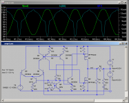
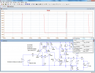
To measure the loop gain, you have to use some kind of probe.
The simplest way when possible is to insert the stimulus between a low impedance output and a high impedance input, see pics.
I have also corrected a few bias problems, which now allow a 0.5 to 11.5V without clipping and a THD level down to 0.0068%
Attachments
I just found out that the harsh clipping sound is caused by the bases of Q5 and Q3 going too low and cutting off Q6/Q7/M1, not by high frequency oscillation  I forgot that changing the degen resistors shifts the bias point.
After fixing the bias, the harsh clipping no longer occurs. There was probably never any high frequency oscillation in the first place.
As for slew rate, I've always understood it this way: slew rate and frequency/phase response are just two ways of looking at the same thing; in the case of an audio amplifier, if the frequency/phase response is ok at full amplitude, then who cares about slew rate?
I did a few spice .trans runs with the input set to 10kHz and 15kHz, and the gain/voltage swing seems to be fine.
I'll implement your suggestions of balanced degen resistors and a feedback capacitor in the pcb build. Right now there is no more space on the breadboard for more components. Gate stopper resistor? I'll probably include a slot for it on the pcb, and only put a resistor on if I experience stability problems; otherwise i'll solder a piece of wire.
The main reason for using 2 input stages is because without the second stage, the input voltage swing only goes down to about 6V. It isn't the THD I'm concerned about.
Anyways, this amp is crap from the point of view of audiophiles, but for my uses it's good enough. Different people have different tradeoffs, and for me the idle power consumption is much more important than audio quality to a certain extent. In my opinion, all parts should be stone-cold when idle. So many commercial amps run with a hot heat sink when idle. I can't hear any difference between this amp and an audiophile-grade amp, so it make no sense for me to optimize THD/slew rate/whatever even further. Before this one I used an amp with a single digit THD for 5 years (also my design) and people even said it sounded good 😀
If you have any ideas of how to design a better amp without trading off low idle power consumption, low voltage operation (+/- 6V), voltage swing, and simplicity, I'd like to hear about it 😀
btw I have the 9540s now so I can try complementary designs too.
I forgot that changing the degen resistors shifts the bias point.After fixing the bias, the harsh clipping no longer occurs. There was probably never any high frequency oscillation in the first place.
As for slew rate, I've always understood it this way: slew rate and frequency/phase response are just two ways of looking at the same thing; in the case of an audio amplifier, if the frequency/phase response is ok at full amplitude, then who cares about slew rate?
I did a few spice .trans runs with the input set to 10kHz and 15kHz, and the gain/voltage swing seems to be fine.
I'll implement your suggestions of balanced degen resistors and a feedback capacitor in the pcb build. Right now there is no more space on the breadboard for more components. Gate stopper resistor? I'll probably include a slot for it on the pcb, and only put a resistor on if I experience stability problems; otherwise i'll solder a piece of wire.
The main reason for using 2 input stages is because without the second stage, the input voltage swing only goes down to about 6V. It isn't the THD I'm concerned about.
Anyways, this amp is crap from the point of view of audiophiles, but for my uses it's good enough. Different people have different tradeoffs, and for me the idle power consumption is much more important than audio quality to a certain extent. In my opinion, all parts should be stone-cold when idle. So many commercial amps run with a hot heat sink when idle. I can't hear any difference between this amp and an audiophile-grade amp, so it make no sense for me to optimize THD/slew rate/whatever even further. Before this one I used an amp with a single digit THD for 5 years (also my design) and people even said it sounded good 😀
If you have any ideas of how to design a better amp without trading off low idle power consumption, low voltage operation (+/- 6V), voltage swing, and simplicity, I'd like to hear about it 😀
btw I have the 9540s now so I can try complementary designs too.
Yes, that is why I changed the 5K to 3.3K.I just found out that the harsh clipping sound is caused by the bases of Q5 and Q3 going too low and cutting off Q6/Q7/M1, not by high frequency oscillation
After fixing the bias, the harsh clipping no longer occurs. There was probably never any high frequency oscillation in the first place.
For a simple signal, full power bandwidth has a direct arithmetic relation with the slew rate, but the reason the two specs exist is because they are not interchangeable generally: when multiple signals are present, depending on their phase the local slew rate can reach higher values than in a simple case.As for slew rate, I've always understood it this way: slew rate and frequency/phase response are just two ways of looking at the same thing; in the case of an audio amplifier, if the frequency/phase response is ok at full amplitude, then who cares about slew rate?
Simply think of squarewave, even with most harmonics rolled-off: a 1V peak squarewave already contains a ~1.5V peak sinewave (Π/2*1V).
Also, the components of the same squarewave can more easily be reproduced if their relative phase is random: it is just a collection of sinewaves of low amplitude, but when the phase is coherent, there will be a high slew rate event two times per cycle.
That is not to say that you need ridiculously high slew-rate to reproduce a band-limited program, it depends on the roll-off profile, etc, but it is prudent to allow for a FPW=twice the bandwidth at the very least, 40KHz for example.
Since it isn't that difficult to reach, it makes little sense to deprive oneself of something so essential
Since you use a single supply, you are not constrained to these 6V for the input stage: you can chose whatever suits you and adapt the FB networkThe main reason for using 2 input stages is because without the second stage, the input voltage swing only goes down to about 6V. It isn't the THD I'm concerned about.
Don't worry: mine are also crap from that point of view, but I try to fix what might be an issue: for example, noise, THD, IMD etc have no clear cut-off point (you cannot define a single fixed threshold below which they become absolutely inaudible). The slew-rate is different: if the amp is operated below its SR threshold, the impact is nil; it is like clipping, except clipping is zero-order and SR first order.Anyways, this amp is crap from the point of view of audiophiles, but for my uses it's good enough.
Of course, when you come very close to the clipping or SR limit, performances begin to degrade, but in a well designed amplifier there is no detectable impact if a few percents of margin remain.
Frequency and phase response are in-between: there is no point reproducing frequencies that no source is able to provide, but strictly adhering to 20 to 20K audio is probably too limited.
Phase response (variations in group delay) are sometimes quoted as inaudible, but that is not that simple: phase information provides cues for spatial localization, and in some extreme cases can have an overwhelming effect: think of the ticking of a clock. It is a weak, but characteristic sound.
If you take the Fourier transform of such a sound, you will end up with a fundamental of say, 1Hz, and a multitude of harmonics extending to many KHz, spaced by 1Hz, all extremely low level. If you reproduce all of these harmonics, but with significant phase deviations, the sound will be become utterly inaudible.
For these reasons, we should not underestimate our auditory system and deliver a best effort whenever possible
Hard-switching class B might be a solution: you use common emitter or source OP's with no quiescent current, and a driver stage designed to switch accurately and rapidly between the two polarities.Different people have different tradeoffs, and for me the idle power consumption is much more important than audio quality to a certain extent. In my opinion, all parts should be stone-cold when idle. So many commercial amps run with a hot heat sink when idle. I can't hear any difference between this amp and an audiophile-grade amp, so it make no sense for me to optimize THD/slew rate/whatever even further. Before this one I used an amp with a single digit THD for 5 years (also my design) and people even said it sounded good 😀
If you have any ideas of how to design a better amp without trading off low idle power consumption, low voltage operation (+/- 6V), voltage swing, and simplicity, I'd like to hear about it 😀
Last edited:
That makes sense, but isn't there a fundamental limit of how high the slew rate of a band-limited amplitude-limited signal can be? I tried looking it up, but couldn't find anything. I did some calculations and I can't seem to find a square wave that when band-limited to 20kHz had a slew rate that exceeded that of a 20kHz sine wave with the same peak amplitude; for example with a 4kHz 1V square wave, its harmonics are:For a simple signal, full power bandwidth has a direct arithmetic relation with the slew rate, but the reason the two specs exist is because they are not interchangeable generally: when multiple signals are present, depending on their phase the local slew rate can reach higher values than in a simple case.
* 4kHz amplitude=1.273V slewrate=32000V/s
* 12kHz amplitude=0.424V slewrate=32000V/s
* 20kHz amplitude=0.255V slewrate=32000V/s
the peak slew rate occurs at the same time for all 3 harmonics, so you can simply add them together to get a peak slew rate of 96000V/s, which is lower than the slew rate of a 1V 20kHz sine wave (125664V/s)
Any math geniuses here would like to figure this out for me? 😀
I'll think about that for my next design.Since you use a single supply, you are not constrained to these 6V for the input stage: you can chose whatever suits you and adapt the FB network
Really? I always thought that if the signal-to-noise ratio or the THD is less than the dynamic range of human hearing (ratio of threshold of pain vs threshold of hearing, 140dB) then you can't possibly hear it.noise, THD, IMD etc have no clear cut-off point (you cannot define a single fixed threshold below which they become absolutely inaudible).
That's true. I once did an experiment of taking the fourier transform of an entire song, randomize the phase of every frequency, and transform it back to time domain. It sounded like every part of the song was mixed together and playing simultaneously.Phase response (variations in group delay) are sometimes quoted as inaudible, but that is not that simple: phase information provides cues for spatial localization, and in some extreme cases can have an overwhelming effect
That makes sense. But I probably wouldn't use 68 ohm gate-source resistors and waste 60mA on just those 2 resistors 😉For these reasons, we should not underestimate our auditory system and deliver a best effort whenever possible
That was what I was trying to do initially 😀Hard-switching class B might be a solution: you use common emitter or source OP's with no quiescent current, and a driver stage designed to switch accurately and rapidly between the two polarities.
How would you design such a driver stage though?
Not me. Fortunately, you can find some ready-to-use info on the net:Any math geniuses here would like to figure this out for me? 😀
Rise time - Wikipedia, the free encyclopedia
For a first order LP the SR is ~1.5 that of a maximum sinewave at the cutoff frequency.
Yes, there is in fact an absolute limit, but it will depend on many factors: the efficiency of your speaker, the colour of the noise, the listening distance, the noisiness of the environment itself, the quality of your ears, etc, etc.Really? I always thought that if the signal-to-noise ratio or the THD is less than the dynamic range of human hearing (ratio of threshold of pain vs threshold of hearing, 140dB) then you can't possibly hear it.
It is simpler to lower the noise floor as much as possible than trying to figure out when it becomes detectable
68 ohm is a bit extreme: this amplifier was meant to reproduce faithfully 100KHz squarewaves, but 5K is at the other extreme.That makes sense. But I probably wouldn't use 68 ohm gate-source resistors and waste 60mA on just those 2 resistors 😉
I think so, but I am not sure I have one that also does rail-to-rail.That was what I was trying to do initially 😀
How would you design such a driver stage though?
I will dig further, but in the mean time, I have found old projects in my archives that could readily be converted by nullifying the quiescent current:
For the first one, the Iq is normally ~50mA, but it can be tweaked down to practically zero without any visible impact on the output. The THD becomes 0.24% instead of the initial 0.22%.
The second one is more complex (don't ask me what I was attempting to do there! 😀), and is already practically zero bias. The THD for this one is 0.034%.
The third is an "autoswitch" scheme. It doesn't fit your bill, because it is not rail-to-rail capable, but it could be used as a driver "engine" for a common-source OP stage
Attachments
- Status
- Not open for further replies.
- Home
- Amplifiers
- Solid State
- custom MOSFET based output stage under development