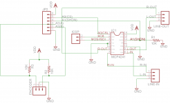
I've build a fairy simple remote volume control device that takes line input signal and using MCP4241 (10K) digital pot changes it's volume. I'm using ATMega MCU to set volume via IR receiver. Basically added remote control capability to the speaker. Audio comes from TiVo or Xbox 360 via HDMI into a Dell monitor which separates audio from it and outputs via mini stereo (3.5mm) plug. Everything works great, except when low frequency sound comes in. It becomes very distorted or clipped (I'm not sure which one, but it sounds like speaker's is getting ripped). This is especially pronounced when playing Xbox (during explosions in the game, for example). I'd like an advice on how I can fix it, and what is actually happening? Is there some kind of filter I can add before digital pot? I'm pretty new to electronics, especially audio...
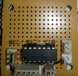
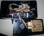
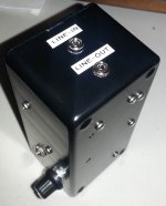
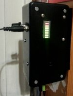
I'm attaching schematic and some pictures of actual device. This is an open source project, I'd love to share it with everyone once I figure out this distortion issue 🙂
I'm attaching schematic and some pictures of actual device. This is an open source project, I'd love to share it with everyone once I figure out this distortion issue 🙂
Attachments
Hi,
the problem could well be, that You are feeding a (non-biased) alternating signal into a single supply circuit.
Think of what happens to the negative going part of Your signal.
You will have to Bias the signal in advance.
If the Datasheet of the digipot doesn't recommend a value choose half the supply value.
Add a series cap of value of ~10uF to the input, feeding into the midpoint of a following voltage divider of 47k+47k. The voltage divider going from Vsupply to gnd.
The joint of cap and VD going to the pots In pin.
Add a similar cap to the output, followed by a Resistor of 100k to gnd.The output signal is then taken from the caps output.
A other possibility could be a second, negative supply if the digipot allows for that.
See the Datasheet.
jauu
Calvin
Some good advice there from Calvin...
There could be a couple of things going on here so here's what I would do. Check Calvins idea. With nothing connected to the input or output terminals, power the device up and measure the DC voltage on those connections. So that is from ground to Rin and Lin, and from ground to Lout and Rout. Vary the volume. Is the voltage on all four points zero ?
If there is DC present then you need to AC couple the device as Calvin suggest.
Also... as you say it does actually work but its the loud bits causing a problem... well that may suggest nothing more than an input attenuator is required. If so then try a 10k in series with each input and a 3k3 from Rin and Lin to ground to make a divider. Values aren't critical, use what you have.
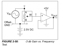
On an IC like this, voltages on any of its pins must not exceed Vdd or go under Vss - which includes the pot. Hence the need for Vdd/2 biasing. (Figure 2-58 in the datasheet shows a test circuit like that.) Inputs and outputs need to be AC-coupled.
Its maximum supply voltage also is 5 V, which means the maximum input level it can accept is 5 Vpp (about 1.7 Vrms, a little short of CD player level but generally sufficient).
I would also consider giving the circuit the luxury of a supply decoupling capacitor. The datasheet (section 8.4) calls for a 100n (usually X7R ceramic), and recommends, "The power source supplying these devices should be as clean as possible."
Reading (or skimming) datasheets in their entirety sometimes pays off. 😉
Thanks a lot for your suggestions guys! I will try it out!
I looked up biasing and I think I get general idea of what it does, but a little confused how.
That schematic in figure 2-58 confuses me... What is ground offset? And why it feeds 2.5V to the ground?
Yeah I'll probably add decoupling cap as well 🙂
I looked up biasing and I think I get general idea of what it does, but a little confused how.
That schematic in figure 2-58 confuses me... What is ground offset? And why it feeds 2.5V to the ground?
Yeah I'll probably add decoupling cap as well 🙂
Hi,
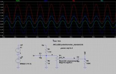
see the waveforms.
V(in) is the input signal swinging pos as well as neg by +-2V (dark-blue).
C1 blocks DC, meaning there may be different potentials on each side of the Cap.
Here, there´s 0Vdc on the left side and +2.5V on the right side.
The +2.5Vdc (black-dashed-line) of V(a) (green) generate from the voltage divider action of R1 over R2 (parallel to P1).
Now the signal swing fits into the ´window´ of the IC´s supply lines, which is 0V and +5V (red).
The signal appears attenuated but with the +2.5V offset at the output of the IC.
C2 DC-blocks, thereby removing the offset again.
R1 references the V(out) to 0V and is a bleeder resistor.
V(out) (light-blue) now is a attenuated copy of V(in).
jauu
Calvin
Attachments

Thank you so much Calvin! One question, why R1 and R2 have these values? If input voltage is 5V after divider I get 4.273V when using 8K2 and 47K... I must be missing something...
Actually Calvin, never mind my previous question (I wish I could edit my posts)...
I was intrigued by your screenshots, and it lead me to discovery of the LTspice. What an awesome program! Reverse engineering of what I saw in your screenshot I was able to run my own simulation (not sure if I did everything correctly) and it appears values of R1/R2 can be almost same (I used R1=1.1K, R2=1K) which brings signal before pot to almost 0V at it's lowest... R3 is a bit of mystery to me tho, removing it doesn't seem to affect V(out) much....
Thanks again, I learned so much today! 🙂 Can't wait to get home and try it on physical circuit!
Attachments
Hi,
You should understand, that You don´t want to ´bring down´ the signal before the pot to almost 0V.
If it worked with 0V offset You didn´t need the whole network in first place.
It must be guaranteed that the sum of the dc-offset voltage and the ac-signal voltage keeps within the allowed voltage window of the Poti-IC, which is between 0V and +5V in this case.
Hence the choice of +2.5V offset voltage as it allows the largest ac-signal voltage swing.
If the offset were set to say +1V and the signal swings could reach +-2V (4Vpp, 2.83Vrms), any signal smaller than -1V would be cut off or distorted.
Rem: as the sim uses a ´real´ poti behaviour, the cutoff action of the poti-IC doesn´t show.
It suffices for the simulation to know that the signal voltage must not fall below 0V and must not exceed +5V.
For a factor-of-0.5 voltage divider action the upper resistor value R1 needed to be the same as the value of the lower part.
Under DC conditions, where C1 is regarded as an open, the lower part consists of R2 and P1 in parallel, resulting in 8.246k.
The small deviation from 8.2k is wholly acceptable as it´d result in a DC-offset of 2.507V.
8.2k, 10k and 47k are easy sourceable standardized values.
Your values are very critical in another point.
A foregoing device has to be able to drive the low impedance load, the poti-network presents.
A minimum value of 2k should allow almost any device to drive the Poti circuit.
The driving device ´sees´ R1, R2 and P1 paralleled.
With Your values these are very low 500Rs.
With the suggested values its 4.11k.
R3 serves mainly as bleeder resistor, that bleeds away the charge stored in C2.
Every cap is a storage for charges.
The charge builds up as the Poti output swings around the dc offset of +2.5V
In that C2 resembles a 2.5V battery .
You know what happens if You connect a battery to a loudspeaker?
As soon as You close the contact a popping sound will happen.
The same will happen with an charged cap instead of a battery.
If You´d hot plug a device to the Poti circuit wo. R3 a voltage/curent pulse can result which may even kill Your speakers.
R3 serves as kind of safety device.
Due to its highish value it has no noteable effect on the signal.
jauu
Calvin
Last edited:
Thanks Calvin!Hi,
Under DC conditions, where C1 is regarded as an open, the lower part consists of R2 and P1 in parallel, resulting in 8.246k.
The small deviation from 8.2k is wholly acceptable as it´d result in a DC-offset of 2.507V.
8.2k, 10k and 47k are easy sourceable standardized values.
Can I use 10K for R1 instead of 8.2K? I don't have any on hand 🙁
Also a stupid question. Does polarity on C1 and C2 matter (I use polarized capacitors)? Since it's audio... If it does which side is more positive near C2? For some reason I'm having hard time understand where electricity flows in that part of the circuit

Whenever you are in doubt over cap polarity (and some circuits genuinely do leave doubt such as feedback return caps in power amps) then I always advice measuring across the part to be sure.
In this case its straightforward (your circuit in post #8 ?) Points "a" and "b" are the positive ends of the two caps.
In this case its straightforward (your circuit in post #8 ?) Points "a" and "b" are the positive ends of the two caps.
Awesome guys!
Just built circuit (with R1=10K) and it works, haven't noticed any distortion yet!
Small issue tho. Now every time I change volume speaker "pops", higher the volume the louder the "pop". When I shut down IC (mute), it also pops. What could it be?
Just built circuit (with R1=10K) and it works, haven't noticed any distortion yet!
Small issue tho. Now every time I change volume speaker "pops", higher the volume the louder the "pop". When I shut down IC (mute), it also pops. What could it be?
I would expect it is because of the DC offset you've just introduced. These volume controllers try to change on a zero cross point to eliminate this issue but it won't be able to do that now (unless you have a strong negative going waveform approaching gnd).
Does somewhat make me wonder how you are supposed to get both distortion free and no pops on volume change with this device 😕 . I shall look at the datasheet later 🙂
Does somewhat make me wonder how you are supposed to get both distortion free and no pops on volume change with this device 😕 . I shall look at the datasheet later 🙂
Ok, there is an example of how you need to connect the device in the datasheet, though it doesn't really show how you'll achieve it:

You need the offset ground, which is shown created with a battery. You can actually create this using the 2x 47k resistors you have now but buffer them using an op-amp buffer. You then have a low impedance 2.5V 'offset ground' or 'virtual ground'. I'd still capacitive couple the input signal, use 3.3-4.7uF or so.
As far as I've seen this device does not actually have zero cross detection, but you shouldn't experience much popping with normal volume adjustments. It'll be a LOT less with this arrangement than what you have now 🙂
Attachments
Thanks Dr_EM!You can actually create this using the 2x 47k resistors you have now but buffer them using an op-amp buffer. You then have a low impedance 2.5V 'offset ground' or 'virtual ground'. I'd still capacitive couple the input signal, use 3.3-4.7uF or so.
Sorry for stupid questions but how would I use op-amp as buffer? Also what kind of op-amp would you recommend?
Thanks a lot! 🙂
Opamp as buffer: Just like in fig 2-58 depicted above (with some supply bypassing as usual). Instead of the wiper, the non-inverting input goes where the 47k resistors from +5V and ground meet. Use a small electrolytic (about 4.7 to 10µ) in parallel with the resistor to ground, otherwise you'd get very bad supply rejection (not to mention higher noise).
The opamp itself must be able to work well on +5V, be unity gain stable and well-behaved with capacitive loading, and not overly noisy. You could use an NJM4556, for example, with its halves paralleled/combined via a few ohms like the O2 headphone amp does. Its current capability seems a little excessive here, but it's a very well-behaved part and won't break the bank.
As signals internally are now referred to +2.5 V, coupling capacitors at the input and output are mandatory in order to get things shifted to 0 V. A high-value pull-down resistor (like 100k) on the 0 V side is considered good practice; it takes up capacitor leakage current in case there is nothing connected and gives a defined potential if the connected device also uses a coupling cap.
Last edited:
- Status
- Not open for further replies.
- Home
- Source & Line
- Analog Line Level
- Bass distortion when using digital pot