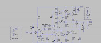
Hello. i am having difficulties in finding phase and gain margin for the amp below.i dont have any problems when finding stability margins for differential input amps but with this singleton input i cant evaluate it on lt spice.maybe its due to the topology used?? can anyone help? Ltspice file is attached.
Attachments
Last edited:
in differential input amplifiers ,i dont have any problem in simulating loop gain,but with this topology i cant....
... anyone help? Ltspice file is attached.
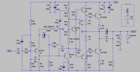
Put a Tian probe on the base of the VAS transistor. After the C1 connection.
This will reveal any instability, actually more correct than the usual methods.
Best wishes
David
its most portable to place any external transistor .model statements directly on the schematic with the Spice directive tool (far right)
Put a Tian probe on the base of the VAS transistor. After the C1 connection.
This will reveal any instability, actually more correct than the usual methods.
Best wishes
David
i will try and report
its most portable to place any external transistor .model statements directly on the schematic with the Spice directive tool (far right)
i will repost .asc file with models on the schematic
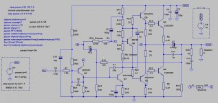
The problem is that there are two feedback paths: one DC for setting the operating point (via R3+Trimmer), and one AC via R10. For AC, both paths are coupled via C3.
One can connect the right-hand sides of R10 and R3, and place the probe between this junction and node A.
Additionally, the input AC voltage source Vin has to be turned of, when feeding the circuit from the gain probe. (it was on!)
Result is OK, ULGF around 300 kHz, phase margin 90 degrees.
Best regards,
Matthias
The problem is that there are two feedback paths: one DC for setting the operating point (via R3+Trimmer), and one AC via R10. For AC, both paths are coupled via C3.
One can connect the right-hand sides of R10 and R3, and place the probe between this junction and node A.
Additionally, the input AC voltage source Vin has to be turned of, when feeding the circuit from the gain probe. (it was on!)
Result is OK, ULGF around 300 kHz, phase margin 90 degrees.
Best regards,
Matthias
the other thing i tried to do last night was to connect the probe between the junction of R20_Trimmer and C3, and Q2's emitter. the results acquired this way were quite logical although i dnt know if the method i used was correct. i will come up with schematics to show you my findings.
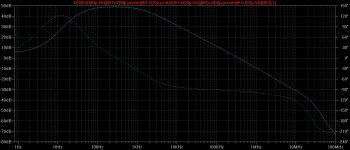
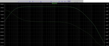
Hi,These were the loop gain results using Tian's loop gain probe.
The results claim 43dB Gain margin and 86 degrees Phase margin but i dont know whether these results are accurate enough or not.
these are the results I got with the other method.
BTW, the circuit contains a subtle problem. According to current terms, one could it call a simple non-symmetrical current-feedback amplifier (CFA), see the CFA threads.
The input impedance at its inverting input (emitter of input transistor) is quite low. I think, currently it is not much larger than the 150R resistor in the feedback network.
So, if you want to increase the loop gain by decreasing the closed-loop gain, you have to take care of the feedback network impedance and also of the coupling capacitor to the emitter of the first trannie.
Kind regards,
Matthias
PS. The way of setting AC 0 for the voltage source Vin is nice!
Last edited:
The input impedance at its inverting input (emitter of input transistor) is quite low. I think, currently it is not much larger than the 150R resistor in the feedback network.
Are you talking about re' which is equal to 25mv/Ic where Ic= collector current of Q2 ?
About coupling capacitor C3 i think that it only affects low frequency closed-loop gain. i dont know if it has a correct value due to the fact that there are 2 feedback paths.
Last edited:
Yes, plus the contribution from (driving impedance at input (R7) divided by beta).Are you talking about re' which is equal to 25mv/Ic where Ic= collector current of Q2 ?
If you probe the loop gain and increase R27 e.g. to 500R, the change will be small. If you reduce, however, R10 to 5k, there will be a larger change.
In order to work properly, the feedback network should have such an impedance, that the feedback voltage is not changed by the loading through the inverting input. The effective input inverting impedance, however, is also scaled by the negative feedback, so it is not as severe as one could conclude from (Ut/Ic+R7/beta).
Matthias
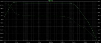
Strange. With my method, i.e. probe between node A and junction between right-hand-sides of R3 and R10, this does not happen.I changed R10 value to 2.2K and R27 to 47 and C3 capacitor to 100uF just for curiosity and then a strange peaking showed up at lower frequencies.What is this supposed to mean?
But there is a difference between our schematics: in yours, the output cap C7 is in the loop. Does increasing its value change anything?
Matthias
the previous schematic on post 13 is the frequency response of the amplifier and not the loop gain.
It is C7. It is part of the feedback loop (probably to reduce its influence on distortion). As its impedance increases at very low frequencies, the feedback decreases. Thus, amplitude a node A increases. If you increase C7, the peak in the closed-loop response vanishs.
Matthias
Matthias
C2, C3, C4 & C7 can each create a single pole roll-off, i.e. high pass filter
If two of them are close in frequency then you get a 2pole filter.
That is where you will see the rise in response followed by the roll-off.
That rise in frequency is an indication of instability.
That is why the passive input filter, C2/R21, should be selected to define the bandwidth of the amplifier.
The problem is that there are two feedback paths: one DC for setting the operating point (via R3+Trimmer), and one AC via R10. For AC, both paths are coupled via C3.
One can connect the right-hand sides of R10 and R3, and place the probe between this junction and node A.
Additionally, the input AC voltage source Vin has to be turned of, when feeding the circuit from the gain probe. (it was on!)
Result is OK, ULGF around 300 kHz, phase margin 90 degrees.Matthias i tested your method and it gives the same results with my method (connecting the probe between the junction of R20_Trimmer and C3, and Q2's emitter.)
C2, C3, C4 & C7 can each create a single pole roll-off, i.e. high pass filter
If two of them are close in frequency then you get a 2pole filter.
That is where you will see the rise in response followed by the roll-off.
That rise in frequency is an indication of instability.
That is why the passive input filter, C2/R21, should be selected to define the bandwidth of the amplifier.Andrew,for passive input filter you mean C4 and R21 ? A ll the other part values (C2,C3,C4,C7) are ok? so what i have to change?
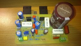
This is the schematic so far and a pcb board for it. All that is missing is miller cap( i only have multilayer type and a 82pF styroflex) ,and vas transistor (i have BD139,2SD669A,KSC3503-D)
How these filters created by C2,C3,C4,C7 should be choosen in ordere to have a good frequency response with n indication of instability. Using the values in schematic the graph seems good enough.
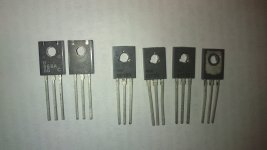
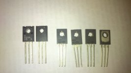
By the way,i suspect that these transistors are fake but i dont know.Have a look.
How these filters created by C2,C3,C4,C7 should be choosen in ordere to have a good frequency response with n indication of instability. Using the values in schematic the graph seems good enough.
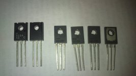
By the way,i suspect that these transistors are fake but i dont know.Have a look.
Attachments

Last edited:
- Status
- Not open for further replies.
- Home
- Amplifiers
- Solid State
- Need help in finding stability margins/loop stability in LTspice for my amp