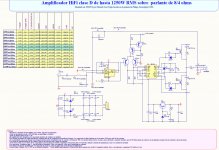
The monster has awoken yet again: http://i.imgur.com/heCHd.jpg
I neatened it up alittle to, its now a inverting setup with feedback from the output.
I neatened it up alittle to, its now a inverting setup with feedback from the output.
And now its happened, the amp was powered up with 2x85VDC from a 1.5kVA transformer, the load was two 4ohm speakers in series for 8 ohms.
A video of the test, yes i was very nervous, this is by far the highest power amplifier i have ever powered up: Big Class D Amplifier - YouTube
I was literally shaking after the test.
A video of the test, yes i was very nervous, this is by far the highest power amplifier i have ever powered up: Big Class D Amplifier - YouTube
I was literally shaking after the test.
Off the point, the song in your video is by Chakra, one of my favourite trance tracks.
Chakra - Home (Original) - YouTube
😀
Chakra - Home (Original) - YouTube
😀
The song in the video was from the "Trance 2000 2nd edition" CD.
I also did a quick power test, into a 2 ohm load, the amp peaked 1800 watts (60V peak into 2 ohms) with the 30 ohm softstart resistor still in series with the transformer primary, it was nice and hot after a few minutes while the amp heatsink was stone cold.
I also did a quick power test, into a 2 ohm load, the amp peaked 1800 watts (60V peak into 2 ohms) with the 30 ohm softstart resistor still in series with the transformer primary, it was nice and hot after a few minutes while the amp heatsink was stone cold.
And now its happened, the amp was powered up with 2x85VDC from a 1.5kVA transformer, the load was two 4ohm speakers in series for 8 ohms.
A video of the test, yes i was very nervous, this is by far the highest power amplifier i have ever powered up: Big Class D Amplifier - YouTube
I was literally shaking after the test.
It works ....🙂
Love the way you did the test Tekko, almost impossible for anyone to see the amplifier parts with that mix, i do believe you were nervous ....🙂
Good one , thats a lot of power ....
...I always thought my workbench would look messy, but your pictures&videos make me feel like a correct german...

Enjoy your beast!
The power is strong with this one.
Let's hope hope that it doesn't turn dark.
Enjoy your beast!
The power is strong with this one.
Let's hope hope that it doesn't turn dark.
I suck at cleaning... Though i dont do much work in the lab nowdays so i guess i dont really bother either.
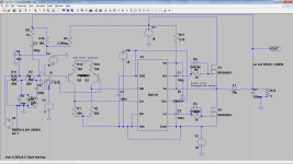
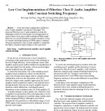
Hello, I am new in Class D, just finishing reading docs from Sony TA-N88, Tripath, Bang & Olufsen IcePower, Philips UcD, Hypex nCore, along with more stuff on www.diyaudio.com and Foros de Electrónica.The circuit is that of my thread "simple class d amplifier". This was never intended as fullrange use, but it still does a fair job.
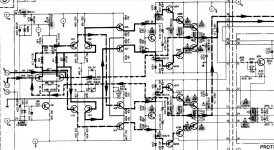
The Philips UM10155 UcD implementation is fascinating me. See attached picture. Clearly they wanted to market the baby basing on discrete components sold by Philips instead of relying on ICs possibly sold by competitors. What helped Philips, is the popular misconception that discrete components will better treat the audio signal, compared to ICs.
As consequence, smart people like Eduardo Tagle (ejtagle) pioneered the IC-way UcD, using a LM311 comparator and a IR2010 MOS gate driver. The resulting PCB is very compact. Are there reliable THD and IMD figures, concerning such implementation ?
Most troubles are coming from the output coil. The recommended choice is the T106-2 from micrometals.
- "T" means Toroid Outside Diameter 26.9 mm
- "106" means Outside Diameter 26.9 mm
- "2" means Iron Powder as core.
AL value (nH/N²): 13.5 - this means that if you wind 100 turns, you will get an inductance equal to 100 * 100 * 13.5nH = 135µH.
Exploding electrolytic capacitors are caused by surplus capacitors. You need up-to-date low ESR capacitors like the ones salvaged from modern computer power supplies (SMPS). Make sure they support the rated DC voltage. Connect them the right polarity. Wear protective glasses when powering up the amp.
I'm curious about the circuit that got presented here.
- Who is the author?
- The frequency gets imposed by the oscillator formed by U3 and U4. What's happening when varying R11 sitting between the filtered output and the audio input?
- What's happening when combining the fixed frequency orientation with some more elaborate feedback?
Do you consider sharing the LTspice simulation file in a .zip, along with the IC and MOS models and subcircuits? In the meantime, I have attached some bits and pieces grabbed on diyAudio, as a starting point. See the attached .zip.
Is it worth opting for a LT1016 replacing the LM311, just like you did in your improved Eduardo Tagle (ejtagle) UcD implementation? Are there reliable THD and IMD figures, concerning such implementation ?
What MOS gate driver IC are you using : IR2010 or IR2110?
I like the fixed frequency arrangement, and I am ready to pay for the added complexity of the fixed frequency implementation if synchronization can be guaranteed, say 8x Fs = 352.8 kHz. How to implement a TTL-level sync input?
Speaking about EMI and RFI, I guess that the most reliable solution is to design a single, compact PCB hosting everything, just like you did for the improved Eduardo Tagle (ejtagle) IC-way UcD implementation. See attached picture.
Reading my post again, I fear it may induce confusion, as it is dealing with :
- the original Philips UcD implementation
- the IC-way UcD implementation pioneered by Eduardo Tagle
- the IC-way UCD improvements suggested by Tekko (and corresponding LTspice simulation, and corresponding PCB), making it very appealing
- the latest schema presented by Tekko (not really an UcD, but ...)
However, having taken the week-end reading lots of stuff relating Class D amps and their pitfalls, I can say that 80% of what's really important, is here and in general, in Tekko interventions.
Quite recently Tekko advised a IEEE publication from 2006, showing a IC-way Class D bridge implementation that could be tweaked in one or another direction like UcD vs. fixed frequency vs. synchronization. See attached pictures. I'm especially interested in building a matchbox-sized compact Class D bridge powered by +19V (unipolar) coming from a 90 Watt laptop power supply, featuring a) the UcD audio quality and b) a TTL sync input for receiving a 8 x Fs clock.
Regards
Steph
Attachments
-
 UcD classddiffcomp1 by Tekko.png69.6 KB · Views: 470
 -
 UcD basicclassdbrd13-1 by Tekko.png80.3 KB · Views: 474
 -
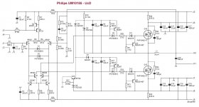
 Philips UM10155 - UcD.jpg96.7 KB · Views: 466
 -
LTspice models and subcircuits by Tekko (diyAudio).zip7 KB · Views: 95
-
 IC-way UcD by Eduardo Tagle (ejtagle).jpg247.4 KB · Views: 468
 -
 schema and simulation.png114 KB · Views: 442
 -
 selfosccswbdmodclassd.PNG97 KB · Views: 244
 -
 IEEE Vol 52 Nov 2006 - Hyoung-Sik Kim.jpg196.7 KB · Views: 241
Wow thats alot of questions which most i simply don't have the equeipment nor knowlege to answer.
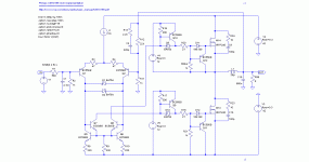
My most recently tried circuit is this: http://i.imgur.com/8xVTPVF.png
Basically an IC version of the Philips circuit, the MAX913 does so far seem to perform better than the LM311.
The clocked class d depicted in this thread was never really intended to be put into actual use, but rather a test to see what i could do with my most powerful power transformer and a set of STE47N50 ISOTOP mosfets, but ended up turning into "lets see how much power i can get outta this thing"
But all work in that project pretty much stopped shortly after my last post in this thread.
As for what gate driver is use, i use mainly IR2010, but have also used IR2110, though the 600V halfbridge voltage capability is overkill for a class d amp.
Hello Tekko, thanks for reacting.
Tekko,
I guess that you are willing to explore Class D, in more aspects. In June 1984 (JAES Volume 32 Issue 6 pp. 415-421; June 1984), Tanaka (and a few other people) from Sansui presented a Fully Balanced Bridge Amplifier. Of course this was an analog design. See attached picture. KVR1 is the usual offset compensation (preventing DC voltage on the load). KVR2 is there for setting the DC operating point (ensuring that both halves operate at half the total power supply voltage).
This weekend, I realized that the differential JFET input stage followed by the Sansui-Tanaka "diamond" stage could be used for implementing a full complementary native Class D bridge, generating the four required gate drive signals.
The two halves of the bridge would inherently oscillate at the same frequency.
The two "diamond" collectors connecting to the negative supply would be loaded by the Philips UcD pseudo-mirror arrangement (Q5,Q6,Q7,Q8 on Philips schematic), sinking current from two NMOS gate drivers (made using Q9,Q11,Q10,Q12 on Philips schematic) connecting to two power NMOS.
Symmetrically, the two "diamond" collectors connecting to the positive supply would be loaded by the same Philips UcD pseudo-mirror arrangement, now using PNP transistors, sourcing current to two PMOS gate drivers connecting to two power PMOS.
I know most people will be repelled by PMOS power devices. There is a price to be paid for full complementary symmetry.
Such design is thus constrained to medium power amplifiers, say +42V and -42V supply rails. Possibly using a single (unipolar) +19V supply coming from a laptop power supply.
I would like to simulate such design. It would help a lot, if you post one or another Class D LTspice .asc (plus .sub and .asy if needed), that is working on simulation.
Any reply welcome.
Time to build a 8th- order passive lowpass filter cutting at 30 kHz, for measuring the spectral purity of the output signal on a PC-based analyzer, along with the power supply rejection. A valuable source for designing such lowpass filter is Paul Bildstein at http://www2.univ-mlv.fr/crmo/fichiers_education/techn_ingen_filtres_actifs.pdfWow thats alot of questions which most i simply don't have the equipment nor knowledge to answer.
I now realize that imgur is a website for sharing pictures. Are you the author of the schematic? It Is there a PCB available? Design files?My most recently tried circuit is this: http://i.imgur.com/8xVTPVF.png Basically an IC version of the Philips circuit, the MAX913 does so far seem to perform better than the LM311.
And ... what's the actual power? Is it stable on a 2 Ohm load?The clocked class d depicted in this thread was never really intended to be put into actual use, but rather a test to see what i could do with my most powerful power transformer and a set of STE47N50 ISOTOP mosfets, but ended up turning into "lets see how much power i can get outta this thing".
Does it imply that you are currently working on another Class D amp?But all work in that project pretty much stopped shortly after my last post in this thread.
Have you compared the IR2010 propagation delay, with the discrete approach taken by Philips UcD?As for what gate driver is use, i use mainly IR2010, but have also used IR2110, though the 600V halfbridge voltage capability is overkill for a class d amp.
Tekko,
I guess that you are willing to explore Class D, in more aspects. In June 1984 (JAES Volume 32 Issue 6 pp. 415-421; June 1984), Tanaka (and a few other people) from Sansui presented a Fully Balanced Bridge Amplifier. Of course this was an analog design. See attached picture. KVR1 is the usual offset compensation (preventing DC voltage on the load). KVR2 is there for setting the DC operating point (ensuring that both halves operate at half the total power supply voltage).
This weekend, I realized that the differential JFET input stage followed by the Sansui-Tanaka "diamond" stage could be used for implementing a full complementary native Class D bridge, generating the four required gate drive signals.
The two halves of the bridge would inherently oscillate at the same frequency.
The two "diamond" collectors connecting to the negative supply would be loaded by the Philips UcD pseudo-mirror arrangement (Q5,Q6,Q7,Q8 on Philips schematic), sinking current from two NMOS gate drivers (made using Q9,Q11,Q10,Q12 on Philips schematic) connecting to two power NMOS.
Symmetrically, the two "diamond" collectors connecting to the positive supply would be loaded by the same Philips UcD pseudo-mirror arrangement, now using PNP transistors, sourcing current to two PMOS gate drivers connecting to two power PMOS.
I know most people will be repelled by PMOS power devices. There is a price to be paid for full complementary symmetry.
Such design is thus constrained to medium power amplifiers, say +42V and -42V supply rails. Possibly using a single (unipolar) +19V supply coming from a laptop power supply.
I would like to simulate such design. It would help a lot, if you post one or another Class D LTspice .asc (plus .sub and .asy if needed), that is working on simulation.
Any reply welcome.
Attachments
Last edited:
Tekko, take a look at the IPW60R070C6 MOSFETs. 3,7nF gatecharge!
further specs: 53A continuous @ 25C and 34A cont. @ 100C.. 159A pulsed. 600Vds, 50V/nS for FET, 15V/nS for Diode.
available and cheap.
further specs: 53A continuous @ 25C and 34A cont. @ 100C.. 159A pulsed. 600Vds, 50V/nS for FET, 15V/nS for Diode.
available and cheap.
Im not an author of anything, my circuits are cobbled together with pieces taken from many different class d schematics, but the whole concept revolves around the Philips UcD circuit.
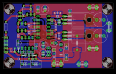
A preliminary board layout for this most recent circuit does exist and is still a work in progress: http://i.imgur.com/0njS4EZ.png
I do remember pushing the BIG clocked class d to about 1800 watts peak when it started to clip, i do however not remember if that was into 2 or 4 ohms.
I am currently working on the UcD concept, as well as investigating the Anaview/Abletec stuff, you can see the basic difference between the two here, based on one of their patents: http://i.imgur.com/HZnDoi4.png
To make a fullbridge class d to be driven from a 19V laptop plugpack i'd use a IC based output stage like the STA505 and equavilents, i've even used TC4422 and UC3710 gate drives as class d output stages with success.
One such UC3710 class d can be seen here, a pre filter feedback(hysteresis) type class d: Self oscillating class D - YouTube and Self oscillating class D - YouTube
Another one using a gate drive ic, only halfbridge though but UcD based with post filter feedback: IXDD430CI class D final update - YouTube
And finally a video of the BIG class d, before the housing work, in this video it is running off of 2x60VDC rails: http://www.youtube.com/watch?v=L7JPrL8gCyY and the full 80+V psu: http://www.youtube.com/watch?v=2uYXpkMnaW4
Last edited:
Looks about right.
powerflux, those fets are not really any better than a IRFP450, almost 4nF gate capacitance is HUGE!
powerflux, those fets are not really any better than a IRFP450, almost 4nF gate capacitance is HUGE!
Tekko, take a look at the IPW60R070C6 MOSFETs. 3,7nF gatecharge!
further specs: 53A continuous @ 25C and 34A cont. @ 100C.. 159A pulsed. 600Vds, 50V/nS for FET, 15V/nS for Diode.
available and cheap.
Trr is 720nS................😀😀😀😀😀
If you know what it is and why it is important.

Trr is reverse recovery, and that mosfet is really slow in that respect compared to a IRFP150N with 180nS, granted tha IRFP150 is 5 times lower voltage rating.
But it is indeed alittle faster than the STE47N50's i used in the BIG class d which has a 1100nS Trr.
The faster Trr the better, ideally this should be 0.000000000000000ps but such mosfet does not exist, unfortunately.
But it is indeed alittle faster than the STE47N50's i used in the BIG class d which has a 1100nS Trr.
The faster Trr the better, ideally this should be 0.000000000000000ps but such mosfet does not exist, unfortunately.
- Status
- Not open for further replies.
- Home
- Amplifiers
- Class D
- Tekko goes crazy