I have simulated and found a difference in harmonic distortion measurement between these two designs...
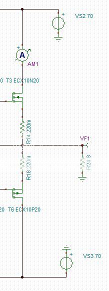
Option 1
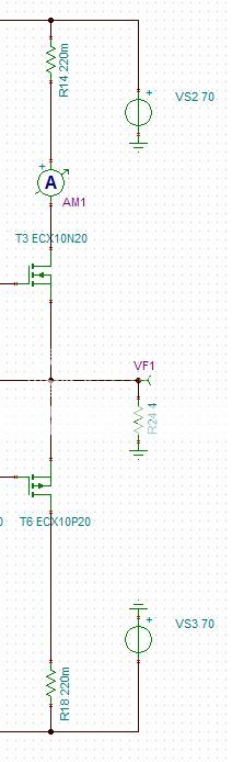
Option 2
Can someone please explain why there is a difference and or what the correct approach is?
BTW Option 2 has the lower Harmonic Distortion figure
Option 1
Option 2
Can someone please explain why there is a difference and or what the correct approach is?
BTW Option 2 has the lower Harmonic Distortion figure
Ever hear of the term 'degeneration'?
Adding source resistors reduces the transconductance of the output stage and makes it a lesser follower, so the total gain is slightly lower. The actual results depend also on the exact way youa re driving the MOSFETs... Moving the source resistors out of the circuit also increases the idle current if you have not compensated for that. Higher idle current gets you higher transconductance and usually more linearity from MOSFETs.
Adding source resistors reduces the transconductance of the output stage and makes it a lesser follower, so the total gain is slightly lower. The actual results depend also on the exact way youa re driving the MOSFETs... Moving the source resistors out of the circuit also increases the idle current if you have not compensated for that. Higher idle current gets you higher transconductance and usually more linearity from MOSFETs.
If it's intended to parallel output devices then source ballast resistors make the requirement for device matching a bit less stringent, but, depending on how you bias the MOSFETS, you will probably need to match them in the arrangement you show, otherwise they may pass different currents.
Hi guys.... Either I don't understand properly or I asked the question badly. I understand the reason for the series resistors and that is to balance the current flowing through different mosfets which are not perfectly matched. I also understand that adding the resistors will reduce the amount of peak current available to source into the load.
What I don't understand is why placing the resistor between the Drain and the supply rail improves harmonic distortion over placing the resistor between Source and the load.
What I don't understand is why placing the resistor between the Drain and the supply rail improves harmonic distortion over placing the resistor between Source and the load.
I'm no expert on FET output stages, but if they work anything like BJT outputs then there is a relationship between the correct resistor value and the quiescent current. The relationship depends on the output stage topology.
You may simply be running with a current which favours a smaller resistor than the one you have. Omitting the resistor may then improve things. Change the quiescent current and you may need a different resistor value. The resistor is not just to limit current; it also plays a role in a smooth handover in the crossover region.
You may simply be running with a current which favours a smaller resistor than the one you have. Omitting the resistor may then improve things. Change the quiescent current and you may need a different resistor value. The resistor is not just to limit current; it also plays a role in a smooth handover in the crossover region.
It only achieves that if the resistors are placed between the sources and the load, as in your option 1.I understand the reason for the series resistors and that is to balance the current flowing through different mosfets which are not perfectly matched......
Adding resistors between the drains and supply rails (as in your option 2) serves no useful purpose - you may as well leave the resistors out altogether.
Agreed.Adding resistors between the drains and supply rails (as in your option 2) serves no useful purpose - you may as well leave the resistors out altogether.
It doesn't even help with current sharing unless the MOSFET is saturated, which isn't the normal operating condition.
My guess is that the lower distortion would exist with no resistor at all. However, this isn't a good idea if you parallel output devices and might just be a simulation fluke.
Ever hear of the term 'degeneration'?
Adding source resistors reduces the transconductance of the output stage and makes it a lesser follower, so the total gain is slightly lower. The actual results depend also on the exact way you are driving the MOSFETs... Moving the source resistors out of the circuit also increases the idle current if you have not compensated for that. Higher idle current gets you higher transconductance and usually more linearity from MOSFETs.
It's not a "fluke"....... and might just be a simulation fluke.
Ilimzn gave you the information.
It only achieves that if the resistors are placed between the sources and the load, as in your option 1.
Adding resistors between the drains and supply rails (as in your option 2) serves no useful purpose - you may as well leave the resistors out altogether.
I don't agree with that statement
godfrey is right; resistors in the drain circuit serve no useful purpose. They simply waste a bit of power, and reduce the peak output.
I'm no expert on FET output stages, but if they work anything like BJT outputs then there is a relationship between the correct resistor value and the quiescent current. The relationship depends on the output stage topology.
You may simply be running with a current which favours a smaller resistor than the one you have. Omitting the resistor may then improve things. Change the quiescent current and you may need a different resistor value. The resistor is not just to limit current; it also plays a role in a smooth handover in the crossover region.
Mosfets are more forgiving towards a specific bias value because the Gm is much less than BJT's and particularly at lower currents, less than a few hundred mA. Bias is typically set at this level so the significant drop in Gm is less pronounced in the output transfer through the crossover region. Source ballast resistors work like emitter resistors, also by smoothing out the temperature coefficient making it easier to thermally track the bias for better thermal stability. A resistor in series with the drain is simply adding it in series with the dependent current source and does nothing. In order to compromise for the optimal bias, Re would be ~= intrinsic resistance of the output transistor at bias current. Because of the significantly lower Gm of the Mosfets at class AB bias, Gm doubling is less of a problem so biasing in a range of 150-300mA is pretty good. If you bias much lower than this, the crossover distortion becomes evident, unless you employ some other sort of linearization technique. Here I you can clearly see the dropout of Gm at the crossing when bias is set to a low value.
- Status
- Not open for further replies.
- Home
- Amplifiers
- Solid State
- Rd or Rs on MOSFET output