The servo is connected to the negative input of the Fet opamp...In LT spice it nulls the offset...
The servo is connected to the negative input of the Fet opamp...In LT spice it nulls the offset...
Miib, the servo you have shown is wrong polarity - needs inverting. This is for sure.
somethings funny...or a little weird... regardless of the connection the modeled servo nulls the offset. If I remove it the offset is 60 mV... hmm
In the design of that buffer have you guys think about adding a battery to the gate of the upper jfet, with less than 1nA of leakage current a litio battery will last forever. And the voltage of source to drain of the lower jfet will be higher .
I like the BF862
I like the BF862
Attachments

I agree that the voltage is too low across drain source. What I do instead, but that takes a few more components, is to use a Zener diode with LP filter, and then a transistor. You can then set VDS to what you prefer.
/S
/S
In the design of that buffer have you guys think about adding a battery to the gate of the upper jfet, with less than 1nA of leakage current a litio battery will last forever. And the voltage of source to drain of the lower jfet will be higher .
I like the BF862
What is the benefit of a higher VDS..?? and Why would you want to create a fixed Cascode..?? then the voltage swing would still have to throw charge so the capacitance comes into play.
Last edited:
In praxis our buffer works very well although the output transistor has only Vgs of the cascode transistor from drain to source.
I Agree.. this is the most transparent buffer I have ever tried...just an impedance converter, to me as transparent as a piece of wire.
Well, to have a fixed VDS is the point 😉
Reasons for higher VDS than VDS = Vp:
1) I can have a VDS that makes the semiconductor sounds best
2) Use a VDS where the JFET is most linear
3) Higher VDS means lower capacitances
Attached are two different ways to cascode for higher than VDS = Vp.
Reasons for higher VDS than VDS = Vp:
1) I can have a VDS that makes the semiconductor sounds best
2) Use a VDS where the JFET is most linear
3) Higher VDS means lower capacitances
Attached are two different ways to cascode for higher than VDS = Vp.
What is the benefit of a higher VDS..?? and Why would you want to create a fixed Cascode..?? then the voltage swing would still have to throw charge so the capacitance comes into play.
Attachments
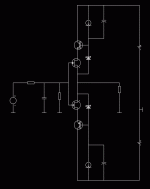
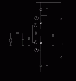
Hmm, the left one is driven as well I would say.Our design is a driven, floating cascode, your design is a fixed cascode, parallel symmetric.
The cascode schematic on the left above, is also a driven cascode if we by driven mean that Vds is locked to the source and not to ground. The cascode I describe above I did not show yet (as it contains rather many components).
BTW,
you need to sort the J310s for Vp as otherwise the cascoded CCS will nto work, right?
/S
BTW,
you need to sort the J310s for Vp as otherwise the cascoded CCS will nto work, right?
/S
Our design is a driven, floating cascode, your design is a fixed cascode, parallel symmetric.
Ugs ( off ) for J310 is between -2 and - 6,5V. If higher voltage over the output Fet is desired the J310 can be selected for highest Ugs. There are N-channel Fets with even higher Ugs. I build our buffer many times and did not select the cascode Fets. Trimming for lowest offset can be done with R29 ( post 635 ).
VDS will not be Vp as I wrote but it will be Vgs as you say. In my simulations, I use a j310 with VP=-3.6V but the Ugs for it is only -2.1V and those 2.1V will be across the lower JFET's VDS.
Source resistors can be used of course and a pot, say 10R, if what I often use to se DC offset when running in open loop.
What I was referring to about the matching need, is that VP for the JFETs in the cascodd CCS cannot be the same but have different and thus have to be selected for VP.
Problem with trimming DC offset with R29 is when you change it, you not only change offset but also the CCS current and thus the current through all the 4 JFETs which in turn changes how low a load the buffer can drive.
BTW, what does R28 (also 220R) do (I usually just connect the gate to the source without any resistor)?
/S
Yes, i would use some source resistors though.
staccatiss, in the buffers that you present in post#649 the capacitors should be parallel with the zeners not with the ccs, I like the idea of using mosfets , but carefull as some mosfet have to much capacitance. the left schema is equivalent to a floating cascode , and is much better than the one from the right. I use this configuration also in some amplifiers.
I am sure it works very well, very good choice of jfet , especially the BF862 that has low capacitance, this buffer can be use with the tagus I/V without any problem.In praxis our buffer works very well although the output transistor has only Vgs of the cascode transistor from drain to source.
Increase Vds will lower capacitance , output impedance , and improve linearity, but i predict that this will be a minor improvements as the BF862 seems to be a good choice. Well done.
smms,
I realized that we need to take care the input impedance next to your circuit.
e.g. SEPP JFET buffer or voltage follower with JFET opamp have high input "resistance" ,but large capacitance.
when the capacitance varies by input signal voltage, the actual IV impedance will vary and cause distortion.
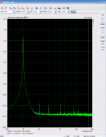
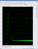
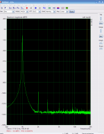
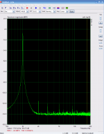
I have made some tests, the conclusion is that as long as we do not use devices with large parasitic capacitances like for example irf510 , there will be no alteration in the linearity. I recommend use floating cascode in buffer to mantain vgs constant, devices like irf510 can be use with floating cascode also.
The first image is without any buffer, second with 2sk146 third irf510 and the last bs170, the output resistence is 1K and 2,5 Vrms all the buffer dont have floating cascodes on purpose. the distortion is measure at the output of tagus.
Attachments
Last edited:
- Home
- Source & Line
- Digital Source
- dac I/V convertion with very low distortion