Could you name a manu of yours devices?
Surprise, surprise, they appear to be UTC the Tiwanese Semi house. The markings are 2N4401-h51 which only shows up related to them. The equipment today is just that good, there is no money in making junk you just need to get devices that are made together.
Last edited:
Scott: Are you going to look at cascoding sinks and sources to improve CMRR as R. Marsh suggests? Thanks Ray
That is possible, I'm going to step through each stage to verify that the extra devices actually make a measurable difference.
Du.uuh! Guru Wurcer dis dun wuk 😡BINGO! The 20Rs on the Output Stage biasing. 🙂
Do we tweak the 20Rs so that with 'no' load (incl. F/B bits so no Iq is lost), there is no voltage between the bases of the 'bias' devices and the output?
Du.uuh! Guru Wurcer dis dun wuk 😡
Don't worry be happy and patient.
This is obvious to some using sims but just in case some arent aware of the practical consequences: In using sim, something that is practical but not appreciated is ---- often the Vbe and diode voltage drop at a design current is very important/critical. You cant always just use a fixed or generic voltage for all.... there can be large consequences between 0.6 and 0.8vdc.... especially when they involve biasing of devices and offsets.
[For the DYI'er reading here, who just wants to build something - it is best not to sub diodes and transistor part numbers. If a 1N914 is spec'ed, don't think that means you can use a 1N4148 instead, for example.] -RNM
[For the DYI'er reading here, who just wants to build something - it is best not to sub diodes and transistor part numbers. If a 1N914 is spec'ed, don't think that means you can use a 1N4148 instead, for example.] -RNM
Last edited:
The JE990 and derivatives with a current-mirrored LTP will balance LTP currents, thus mimimizing offset automatically. Any slight residual imbalance in DC currents is taken care by the inductors across the degeneration resistors, which ensures that the LTP emitters/sources are at nearly identical DC voltages, regardless of any DC current mismatch in the two legs of the LTP....SW-OPA seems inordinately sensitive to the transistor models used and also their Iq.
...
The offset voltage changes up to more than 4V with different BJTs, FETs and small changes in Iq for input & output stages.
... the imbalance in the input device currents ...
...the FET990 circuit is far more tolerant and output offset changes much less with different transistors & Iq.
I tried the inductor trick in the SWOPA-SE (single-ended, 8-BJT), and it works - but the behaviour into hard clipping is much worse with inductors in the LTP. So out it went, though I'll revisit it later if necessary...
Edit: Typical LTP inductor values are between 1 and 50 uH. TDK makes them in 0603, 0805 and 1206.
Of course, the LTP inductor trick changes the AC response, and compensation has to be adjusted accordingly.
Last edited:
linuxguru! Do not take the name of Guru Wurcer (aka Lord Shiva) in vain! Your single-ended 8-BJT circuit has never been blessed. 😡I tried the inductor trick in the SWOPA-SE (single-ended, 8-BJT) ..
Though my circuit is derived from one of Guru Wurcer's ideas, I'm careful to call it FET990 as I've made substantial changes so it may no longer have his blessing. 😱
what's the difference?............. If a 1N914 is spec'ed, don't think that means you can use a 1N4148 instead, for example.] -RNM
I hold both in stock and thought whichever comes out first I use !
linuxguru! Do not take the name of Guru Wurcer (aka Lord Shiva) in vain! Your single-ended 8-BJT circuit has never been blessed. 😡
Though my circuit is derived from one of Guru Wurcer's ideas, I'm careful to call it FET990 as I've made substantial changes so it may no longer have his blessing. 😱
OK calm down. The problem is the Is for the 1N914 seems to be random in all the model files I've seen and does not match the transistors. Sorry for the oversite, we don't have separate diodes they are always diode connected transistors.
Open the LTSPICE model files you will notice that the 1N914 and 1N4148 have exactly (to 3 digits) the same values for most parameters which is obviously nonsense. Usually it simply does not matter.
Best fix is to use diode connected transistors for just D3 and D5.
BTW the best place to trim offset is at R16 and R17 with a pot, wiper connected to the rail. 10k or 20k should be fine.
Back to my breadboard, after my 9 holes (it IS Saturday after all).
Last edited:
For the DYI'er reading here, who just wants to build something - it is best not to sub diodes and transistor part numbers. If a 1N914 is spec'ed, don't think that means you can use a 1N4148 instead, for example.
No difference.
"The 1N4148 replaced the 1N914, which had a much higher leakage current (5 microamps vs. 25 nanoamps). Since leakage is almost never a desirable property, today manufacturers produce the 1N4148 and sell it as either part number"
Source: Wikipedia
Open the LTSPICE model files you will notice that the 1N914 and 1N4148 have exactly (to 3 digits) the same values for most parameters which is obviously nonsense.
Hahaha I learned this issue the hard way

What IS sometimes significant is that we might assume that 4148-style diodes have precisely the same I-V characteristics as diode-connected transistors. They do not, but it many applications the difference is of little importance. But the I-V curve for operation of the diode in the injection region, i.e., forward-biased significantly, will differ from that of a diode-connected transistor. This is discussed in many references* and for empirical data on differences among diodes see the Appendix E table in Pease's book Troubleshooting Analog Circuits, pp. 196-198. There is also a chapter 6, Understanding Diodes and Their Problems, which at least mentions "high-level injection" without showing the modification of the diode equation that it entails. Sadly, Pease omits the diode-connected transistor, and as well doesn't mention most of the manufacturers of the DUTs.
There was an Ideas for Design or some such years ago in which the author linearized a transistor gain stage by use of a diode. When I saw it I thought Ah, why not a diode-connected transistor? But it didn't work --- without declaring such, the circuit worked by virtue of the I-V curve differences, not their similarity 🙂
Brad
*including everyone's favorite compendium by Horowitz and Hill, except I can't locate it in the second edition right now.
See 4.4.4 and the rest of this reference where the modifying term eta, high injection, and the effects of series resistance are discussed in greater depth: The p-n diode current . The latter says you don't see much of the high-injection region separate from the series-resistance-dominated region, which is an assertion to be questioned 🙂 Note that the ideal region is shown as below 550mV at room temperature for a typical small-signal diode, which is rarely where we operate them.
A quick observation. Most folks have a little handheld VOM with a diode check function which works by forcing a current and measuring the drop. Simply test a 100 Ohm resistor and you know the test current (V/R) mine uses 1mA. You can use this to guestimate the saturation current of your batch of diodes/transistors from the diode equation and fine tune your sims.
I just grabbed 3 1N4148's from the junk bin and at 1mA they measured .653, .654, and .656 volts while my batch of 2N4401's measures about .655 volts connected as diodes.So clearly the stock models are off and this explains why Pete B's JE990 sim was so far off on bias, in fact the diodes are pretty close to the transistors.
EDIT - be careful not to heat the devices by holding them
Last edited:
Twitchy SW-OPA?
One was at 0.8mA with BC556c and the other at 4mA with 2sc2362. In both cases, 1n4148 had significantly bigger drop. In the 4mA case, requiring a 180 resistor instead of 200 on the 2sc2362 emitter; ie 80mV
This bears on my investigation into twitchy SW-OPA. ricardo.txt which I uploaded in #1949 has BJT models from several gurus. I have 2 sets of c2240/a970 and also 4401/3.
Scott's c2240 has some 100mV more Vbe than his a970 at the same current.
Cordell's 4401/3 have closer Vbe than fas42's but for some reason results in a lot more THD in some circuits. I've looked at *.log which LTspice produces on .opt analysis cos this gives stuff which I pretend to unnerstan. The only difference which stands out is Ro whatever that is.
My own Jurassic experience with 2240/970 is that the models with closer Vbe are closer to real life.
I've also increased RB to more believable values in preparation for noise analysis but that shouldn't give 100mV errors. I'll take them out & see if that makes a diff.
Guru Wurcer, I'd still like to know if your instruction to adjust for 8mA applies to the output devices or just to the 4R7 resistors.
I've used 1n4148 in place of diode connected transistors for simple current mirrors in a production amp so have a lot of data on 2 cases.I just grabbed 3 1N4148's from the junk bin and at 1mA they measured .653, .654, and .656 volts while my batch of 2N4401's measures about .655 volts connected as diodes.So clearly the stock models are off and this explains why Pete B's JE990 sim was so far off on bias, in fact the diodes are pretty close to the transistors.
One was at 0.8mA with BC556c and the other at 4mA with 2sc2362. In both cases, 1n4148 had significantly bigger drop. In the 4mA case, requiring a 180 resistor instead of 200 on the 2sc2362 emitter; ie 80mV
This bears on my investigation into twitchy SW-OPA. ricardo.txt which I uploaded in #1949 has BJT models from several gurus. I have 2 sets of c2240/a970 and also 4401/3.
Scott's c2240 has some 100mV more Vbe than his a970 at the same current.
Cordell's 4401/3 have closer Vbe than fas42's but for some reason results in a lot more THD in some circuits. I've looked at *.log which LTspice produces on .opt analysis cos this gives stuff which I pretend to unnerstan. The only difference which stands out is Ro whatever that is.
My own Jurassic experience with 2240/970 is that the models with closer Vbe are closer to real life.
I've also increased RB to more believable values in preparation for noise analysis but that shouldn't give 100mV errors. I'll take them out & see if that makes a diff.
Guru Wurcer, I'd still like to know if your instruction to adjust for 8mA applies to the output devices or just to the 4R7 resistors.
Checking in --- good to see expansions on real world build issues discussed in the Vbe and diode drops/I-V et al. One of the reasons I measure so often rather than relying soley on models ---- Sophisticated programs which use known processes and known results of those processes are not in my domain. I measure at the same voltage/current I will be using the part.... and again for same P/N but different brand... no assuumptions. If you don't, the results can be all over the map. We want repeatability for the DIY'er to make and enjoy the fruits of this labor of love.
Last edited:
Note that the ideal region is shown as below 550mV at room temperature for a typical small-signal diode, which is rarely where we operate them.
Easy experiment take two that are close and parallel them the transistors show the expected 18mV drop but the diodes don't. Again you can probably predict close to what you want with just a VOM.
Somewhere back in ancient times I posted data from a bunch of 4148s, not sure if it was in here. They were off of the same taped batch, not sure of the manufacturer. I taped them to a paper and went down the row touching them only with the Fluke 8062A DVM with the 1mA excitation. The distribution of forward voltages was pretty tight, although a hint of bimodality.Easy experiment take two that are close and parallel them the transistors show the expected 18mV drop but the diodes don't. Again you can probably predict close to what you want with just a VOM.
Anyone know what Ro is?I've looked at *.log which LTspice produces on .opt analysis cos this gives stuff which I pretend to unnerstan. The only difference which stands out is Ro whatever that is.
The 3 online SPICE references don't mention anything at all so this might be only LTspice.
Somewhere back in ancient times I posted data from a bunch of 4148s, not sure if it was in here. They were off of the same taped batch, not sure of the manufacturer. I taped them to a paper and went down the row touching them only with the Fluke 8062A DVM with the 1mA excitation. The distribution of forward voltages was pretty tight, although a hint of bimodality.
A quick experiment measuring 1, 2, and 3 matched diodes in parallel gives about 35 Ohms series R so they behave "ideally" only up to 10's of uA.
Anyone know what Ro is?
The 3 online SPICE references don't mention anything at all so this might be only LTspice.
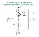
http://people.seas.harvard.edu/~jones/es154/lectures/lecture_3/bjt_models/bjt_models.html
Attachments
Last edited:
- Home
- Source & Line
- Analog Line Level
- Discrete Opamp Open Design