Typically they're scribed on a sheet of heat activated sticky plastic and stretched. Now they would probably use a vacuum pencil pick and place after that.
The same die dual issue would be what is the substrate, I thought it might be the back gate so isolated duals would have to be two die. We always bought them that way.
EDIT Sorry EUVL the FET's were drawn funny, and some symbols show the arrow at the drain.
I ran across a company in Utah making four-terminal JFETs with front and back gates. They seemed to be focusing on the X-ray spectroscopy biz to begin with, branched out into FETs. One "package" shown was a "nailhead". Your business to select a low-loss dielectric 🙂
The paper was in the Hewlett-Packard Journal (...)
February 1971 issue: http://www.hpl.hp.com/hpjournal/pdfs/IssuePDFs/1971-02.pdf
L.
How nice that is available! Thanks for finding it.
Brad
How nice that is available! Thanks for finding it.
I must confess I'm addicted to HP journal 🙂
L.
How nice that is available! Thanks for finding it.
Brad
All math no simulator, interesting look at old school analysis. The old Teledyne publications were also good in this respect.
All math no simulator,
On a 9100A - a ~20 kg RPN programmable calculator with a 196 steps wide program memory 😱
L.
I ran across a company in Utah making four-terminal JFETs with front and back gates. They seemed to be focusing on the X-ray spectroscopy biz to begin with, branched out into FETs. One "package" shown was a "nailhead". Your business to select a low-loss dielectric 🙂
Are there dual gate jFET's similar to a dual gate MOSFET?
-RNM
No, those were front and back gates. Not a cascode structure.Are there dual gate jFET's similar to a dual gate MOSFET?
-RNM
EDIT: Actually I think there were some integrated cascode duals, but they didn't being out all the connections.
Last edited:
2SK2145, the ratings/specs are for devices in parallel operation or single devices?
Afaik not all jfets can be run "backwards"... most?
...then the question is the IDSS group 1/2 of the parallel IDSS or??
So, what is the application for a dual jfet with the sources tied together - or why not internally wire them in parallel and offer the device as a "single"?
Afaik not all jfets can be run "backwards"... most?
...then the question is the IDSS group 1/2 of the parallel IDSS or??
So, what is the application for a dual jfet with the sources tied together - or why not internally wire them in parallel and offer the device as a "single"?
Here's a nice input diff stage device, but doesn't give its best performance with +/- 15 VDC supplies: (and p-channel devices aren't possible in this part of the galaxy, at least)
http://www.triodeel.com/6dj8_p3.gif
Thanks,
Chris
http://www.triodeel.com/6dj8_p3.gif
Thanks,
Chris
Last edited:
Sorry... lost in space again... basic LTP... thinking of the drains tied in my head... my brains tied in knots, same thing.
_-_-bear
Scott,
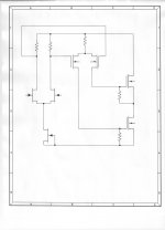
A SMD dual JFET in SOT23 is too good for me to give up, so I went back to the Toshiba website.
It says (see attached) internal connection common source.
So it can at least be used for input LTP.
Toshiba never says whether their FETs can be used with D/S swap.
All the ones I tried can, even though some has a slightly different Idss when reversed.
But this is solvable even if the lower FET has lower Idss when reversed.
Just tie a resistor or a CRD from Vout to the negative rail.
So I am still on for this one.
I think Dave posted the wrong link.
Here is the link to John's circuit using N-JFETs as input.
http://www.diyaudio.com/forums/anal...discrete-opamp-open-design-4.html#post3138300
And I also put it here.
I'll do a PCB layout in SMD. I like this.
Patrick
Attachments

Hi Patrick,
Just an example for the LTP application... I agree this one John posted with MOSFET VAS is much more interesting. Looking forward to it.
Dave
Just an example for the LTP application... I agree this one John posted with MOSFET VAS is much more interesting. Looking forward to it.
Dave
John,
Would you be so kind to pick a Dual P-MOS for the second stage, before we get Spice models for simulation ?
(Had to add the last one separately as I exceeded max file size for Zip.)
Thanks,
Patrick
Would you be so kind to pick a Dual P-MOS for the second stage, before we get Spice models for simulation ?
(Had to add the last one separately as I exceeded max file size for Zip.)
Thanks,
Patrick
Attachments
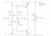
What would you expect from a configuration like this?
The input stage does not need additional components for biasing.
It will offer high input impedance and low noise.
R1 and R2 allow adjustment of bias independently from adjustment
of gain and degeneration which is solved by R3 and R4....
Last but not least you could use such an OP amp for voltage feedback configurations and current feedback applications as well. In current feedback applications one could use the nodes of R1 as current feedback inputs, or center tap R1...
All the rest of the circuit is mostly standard.
Attachments
- Home
- Source & Line
- Analog Line Level
- Discrete Opamp Open Design