well, try this...
Much of the discussion on this thread revolves around a set of documents that Dario has placed on a Google Documents page:
https://docs.google.com/#folders/0B-qKRBuaKtzYYWNkNzRmODktZTQyNS00YjA2LWIwNzItN2UzNzhjODI5MWRm
[or see links Dario has placed, for example, page 113 , message 1125]...
By creating the Google Docs folders, we have a single place where you can find the BOM's schematics and pictures, and know that you're looking at the most recent updates.
Paul
no, not really
Much of the discussion on this thread revolves around a set of documents that Dario has placed on a Google Documents page:
https://docs.google.com/#folders/0B-qKRBuaKtzYYWNkNzRmODktZTQyNS00YjA2LWIwNzItN2UzNzhjODI5MWRm
[or see links Dario has placed, for example, page 113 , message 1125]...
By creating the Google Docs folders, we have a single place where you can find the BOM's schematics and pictures, and know that you're looking at the most recent updates.
Paul
hi a little of topic but not much.
I have received some parts for the DAC from Distrelec with an invoice.
There is no indication of how to pay, how do members generally pay.
I am in the UK🙂
I have received some parts for the DAC from Distrelec with an invoice.
There is no indication of how to pay, how do members generally pay.
I am in the UK🙂
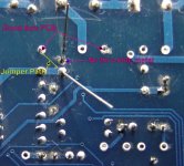
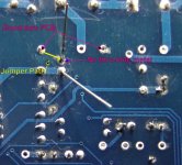
In my upgrade process I unfortunately lost some thru-hole metal sleeves again. 😡
The signal paths are not much of a problem and some of the grounds are repairable by flowing solder up the lead to the top of the board.
Will I be creating a problem by jumpering to the closest "valid" ground/- position on the bottom of the PCB?
The signal paths are not much of a problem and some of the grounds are repairable by flowing solder up the lead to the top of the board.
Will I be creating a problem by jumpering to the closest "valid" ground/- position on the bottom of the PCB?
Attachments
In my upgrade process I unfortunately lost some thru-hole metal sleeves again. 😡
I'm sorry to hear that...
Will I be creating a problem by jumpering to the closest "valid" ground/- position on the bottom of the PCB?
So the broken via is a ground connection?
If so I think it would be fine.
Hi Dario, Yes it is ground. The few signal pads that were lost can easily be fixed by scraping the trace and applying solder to reconnect.
....and thank you for not reminding me about the rework station you recommended several pages ago.
....and thank you for not reminding me about the rework station you recommended several pages ago.
Hi Bob,
I've done the same, bent the lead around to the next ground point to fix.
I don't like the modern idea of two layer boards, give me the old ones with all tracks on the bottom any day🙂
I've done the same, bent the lead around to the next ground point to fix.
I don't like the modern idea of two layer boards, give me the old ones with all tracks on the bottom any day🙂
In my amplifier (Yamaha DSP-A1) there are some DAC chips. All of them are AK4324. That is a 1 bit DAC, 128 times oversampling up to 96 kHz. 24 bit, 8 x digital filter and SCF filter in the analogue part.
So what is a better solution? Keep my S/P DIF output of the CD player (and have the Yamaha process it), or use the mini 2496 DAC board (which I now installed in the CD-player), and use the analog output to the amplifier?
The Yamaha is already 12 years old, so is the technology. Or is the technology in the AK4324 chip still "acceptable", compared to the 2496 mini DAC?
Your PCB hyperlink seems to be a picture of a different board to the pcb discussed here.
I'm no expert but it has different chips in different places.
Also your board has an USB input....
Bill
I'm no expert but it has different chips in different places.
Also your board has an USB input....
Bill
Last edited:
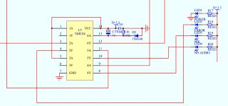
I have a quick questions for those who bought only the pcb. Bottom left corner shows 10k R, while it's 100k on the scheme I've got from supplier. What value should I use?
This picture is for a board, with USB support. Basically it is the same, but still different.
Has anyone determined a preferred spec (part number) for the on-board LEDs ?
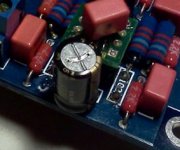
Also, C40 and C42 are listed in the upgrade BOM but are not installed in the picture from the Goggle Docs ?????
Also, C40 and C42 are listed in the upgrade BOM but are not installed in the picture from the Goggle Docs ?????
Last edited:
Also, C40 and C42 are listed in the upgrade BOM but are not installed in the picture from the Goggle Docs ?????
They are at the bottom side of the board.
If you look closely you can see the leads sticking out on top of the board
regards
Attachments
Last edited:
Should a new thread be started for the USB (CM102S) variants of the board?
I've got one on order with the CS8416 + CS4398.
From looking at the schematics it seems to me that there are about five variants of these boards using the CS8416. All use basically the same power supply and output filter with component value variances.
In general, mods to one are applicable to any of the others with the exception of the output DAC having different features (especially the pinout changes for the CS4398 vs AK4393 and AK4396).
I realize the thread was started specifically for the AK4393, but it evolved to encompass the AK4396 as well, so it seems to make sense to include the newer AK4398 boards as well.
What makes sense to me may not agree with the OP, so I am asking before posting more on the AK4398.
Respectfully,
Steven
thanks a lot!
then probably I would use your reg - LM317+BD139 + U6 for A+3.3 part.
I've got the parts for PS finally and curious now, is it safe to omit U6 at all, I mean if I stay with simple shunt from Dario (LM317+BD139+zener) could I directly feed CS8416 A+3.3 bearing in mind voltage peaks during switching on/off the dac?
- Home
- Source & Line
- Digital Line Level
- DAC 2496 (AK4393) DAC KIT With CS8416+AK4393+5532