now ...wahab obviously we are missing something here .
A bias resistor (with a paralleled cap) for the drivers, from the emitter of Q10 to emitter of Q11. I'd do about 30-40mA, 1.2V/40mA = 30R. 33R, a common value, would make ~ 36mA. stick a small heat sink on them.😉 If you are going to build, make sure to fix the Vbe multiplier pot so the wiper does not go to the base of Q9.
Some thoughts, IMO:

You might get away with a smaller VAS. 4mA ought to drive the drivers, even at 40mA. To keep simple thoughts, if beta is at least 40, that's only 1mA of base current. 40V X 4mA = 160mW average, 400mW peak, you could use TO-92 small signal devices.😉 You might throw a resistor in series with the base of Q8, in case Q8 were to saturate if driven to clipping it would not affect the bias setting for the IPS CCS, Q3. This circuit might be a candidate for TMC.

Last edited:
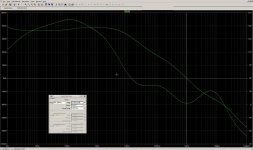
All is not lost. I made a few small changes and the performance is now very respectable.
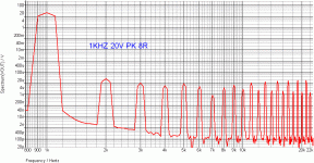
THD for 70W into 8 ohm is
0.000776% at 1kHz
0.004688% at 20 kHz
The clipping behaviour isn't quite exemplary, but maybe I expect too much. Any thoughts on this?
The circuit _seems_ to be stable, but I haven't crunched the numbers for that yet. Will do so tomorrow.
THD for 70W into 8 ohm is
0.000776% at 1kHz
0.004688% at 20 kHz
The clipping behaviour isn't quite exemplary, but maybe I expect too much. Any thoughts on this?
The circuit _seems_ to be stable, but I haven't crunched the numbers for that yet. Will do so tomorrow.
Attachments
Last edited:
Member
Joined 2009
Paid Member
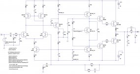
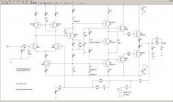
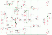
Interesting design (post 1).
The output reminds me a little bit of the KRILL amplifier by Steven Dunlap - you have the drivers connected directly to base of the output devices with no connection between the bases of the output devices. This means that minority charge carriers left behind when the power devices switch off (this is class AB right?) have nowhere to go. It is the feature of the KRILL that caused a huge stir in the relevant threads and is credited with a nice sounding amplifier despite the controversy.
Another interesting feature is the compensation. You have a resistor in series with Cdom. I've ready about the benefits of this approach and wondered why nobody does it.
You have a high gain LTP because you are using current mirror load. But you haven't used emitter degeneration in the LTP devices. I also don't use these on my TGM1 amplifier, but I have very little gain to 'throw away' on degeneration. You have plenty of gain, why not use some degeneration. It has many benefits.
Some base stoppers for the driver devices perhaps ? (100R should be fine)
No rail decoupling for front end from power output ?
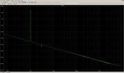
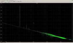
Ingenious - your first FFT plot has too high a 'noise floor' and spikes are inverted - it's not good enough to show proper results. You need to let the simulation run longer so that the capacitors in it reach final values and noise floor is pushed down to show full FFT profile; any time you have FFT spikes pointing down is a sign that your simulation is inadequate. Also I like to add 0R5 internal resistance to the 'batteries' to show realistic power supply impedance, especially when exploring the details of behaviour under extreme conditions such as clipping into low impedance loads.
The output reminds me a little bit of the KRILL amplifier by Steven Dunlap - you have the drivers connected directly to base of the output devices with no connection between the bases of the output devices. This means that minority charge carriers left behind when the power devices switch off (this is class AB right?) have nowhere to go. It is the feature of the KRILL that caused a huge stir in the relevant threads and is credited with a nice sounding amplifier despite the controversy.
Another interesting feature is the compensation. You have a resistor in series with Cdom. I've ready about the benefits of this approach and wondered why nobody does it.
You have a high gain LTP because you are using current mirror load. But you haven't used emitter degeneration in the LTP devices. I also don't use these on my TGM1 amplifier, but I have very little gain to 'throw away' on degeneration. You have plenty of gain, why not use some degeneration. It has many benefits.
Some base stoppers for the driver devices perhaps ? (100R should be fine)
No rail decoupling for front end from power output ?
Ingenious - your first FFT plot has too high a 'noise floor' and spikes are inverted - it's not good enough to show proper results. You need to let the simulation run longer so that the capacitors in it reach final values and noise floor is pushed down to show full FFT profile; any time you have FFT spikes pointing down is a sign that your simulation is inadequate. Also I like to add 0R5 internal resistance to the 'batteries' to show realistic power supply impedance, especially when exploring the details of behaviour under extreme conditions such as clipping into low impedance loads.
Last edited:
Ingenious - your first FFT plot has too high a 'noise floor' and spikes are inverted - it's not good enough to show proper results. You need to let the simulation run longer so that the capacitors in it reach final values and noise floor is pushed down to show full FFT profile; any time you have FFT spikes pointing down is a sign that your simulation is inadequate.
Thanks, I have run the simulation for longer. The result is attached.
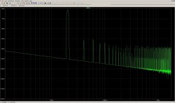
The only way to get rid of the sloping FFT 'noise floor' (that I know of) is to take the low frequency caps out of the circuit before running the simulation, but some would call that cheating. 🙄
Attachments
Last edited:
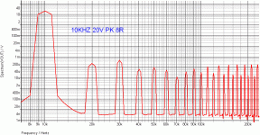
Thanks, I have run the simulation for longer. The result is attached.
The only way to get rid of the sloping FFT 'noise floor' (that I know of) is to take the low frequency caps out of the circuit before running the simulation, but some would call that cheating. 🙄
The other way is to run your sim for a much longer time, perhaps 500 - 1000 ms. start saving at 400 and finish at 500 and see what you get 🙂 depending on how long it takes for the DC to stabilise it might even need a few seconds.
Tony.
Last edited:
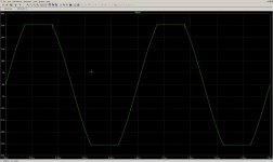
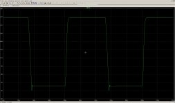
And the 20kHz square output. Slew rate is ~15V/us for the negative slope and ~30V/us for the positive slope.
Attachments
Last edited:
Interesting design (post 1).
Another interesting feature is the compensation. You have a resistor in series with Cdom. I've ready about the benefits of this approach and wondered why nobody does it.
Look here first pdf is schematic, TCM is used and resistor in series with Cdom.
http://www.diyaudio.com/forums/solid-state/182554-thermaltrak-tmc-amp-5.html#post2856542
dado
- Status
- Not open for further replies.
- Home
- Amplifiers
- Solid State
- Anybody willing to simulate ?