John, Anand - thanks guys.... I'm just glad it's over and can tidy up the dining room table! (oh, and that it sounds as good as hoped or expected too)
Wow, Caddock XLR's, FPE/Schaffer, etc...state of the art build, congrats.
Anand.
Sorry I meant Cardas XLRs!
Anand.
See Mez boards on the DIYA store.
I saw that before I saw this thread and was wondering if there where the Blue Edition PCB's I looked through the group buy forum and didn't see a thread there.
The Hypnotize Hot Rod DCB1 was a special single route board for those looking for straight modules, putting together either a balanced one, or just to buffer a stereo route, wanting no full preamp facilities in general, maybe because they already had an input or optical volume module, good mech switch etc. The Mez can be chopped down to ~Hypno and its always available. The Hypnotize from time to time built some ~50pcs minimum production demand and if possible I ask Tea-Bag to combine when there is a reg shipping out etc. But I don't think it catches any momentum anymore. Maybe he has a couple of spares, don't know.
Thanks Salas
No worries I can get the other PCB not problem just need two of the inputs I will just bypass the others. I want to compare it to my B1.
Regards
Dave
No worries I can get the other PCB not problem just need two of the inputs I will just bypass the others. I want to compare it to my B1.
Regards
Dave
You probably didn't mix them up. To find the pair orientation one must test them.
Selecting for Idss is sufficient for B1 and DCB1, but the simple Idss test is not accurate enough if you are looking for pair matching.
Set up a plug board.
Get ready to apply 20V,0V to it.
Connect one of the selected pair as a CCS, i.e. short Gate to Source.
Connect 0V to this Source/Gate
Connect the other with 1k (or 100r) across Gate to source.
Connect it Source to CCS Drain
Connect +20V to the top Drain.
Measure the voltage across the 1k0 resistor. Black probe to Source end and red probe to Gate end. This measurment is the Vgs of the upper device and should be very close to 0.0mVdc. If there is a small offset, this is th eoutput offset of the DCB1.
If the Vgs is +ve then you have the order as required to go into the DCB1. If the Vgs is slightly +ve, then swap the two FETs around. The Vgs should now be slightly -ve. This is the order they get fitted into DCB1.
As an alternative solder a 6pin 0.1" pitch SIL socket into the DCB1. Now you can test on the DCB1 PCB and at the Voltages of the DCB1.
Are you sure about the 1k resistor? With the resistor I always measure 0 V , even with the most mismatched. without the resistor it behave like you say.
D.
Sent from my N-04C using Tapatalk
Is there any advantage in replacing the 2sk170-BL with the 2SK369-V ? Do I have to change the psu?
D.
D.
You will gain in linearity due to large Yfs, you will lose bandwidth due to large Ciss, you will need TO-92 sinking due to large IDSS. You will want even less source impedance (small volume pot) to stay ''fast''. PSU can take much more, no need changing.
P.S. Your stash is now targeted by the unobtainium FET Pink Panther team.
P.S. Your stash is now targeted by the unobtainium FET Pink Panther team.
🙂 You can find nice stuff here in Japan, sometimes.
Andrew, another think that I noticed is that inverting the order of two JFET, with similar Idss on the measurement setup you recommended, in one case you have higher Vgs then in the other case, but the value is always positive. I guess the right order is the one with the lower value.
Thanks,
Davide
Andrew, another think that I noticed is that inverting the order of two JFET, with similar Idss on the measurement setup you recommended, in one case you have higher Vgs then in the other case, but the value is always positive. I guess the right order is the one with the lower value.
Thanks,
Davide
Let me see if I got it right:
1) The lower jfet is the CCS, in the mesmerize board these are the external JFET.
2) The CSS sets the current for the upper JFET.
3) The upper JFET should run at a current that is not larger than his Idss.
4) So that's why we want the lower Idss device to be the CSS (Lower in the schematic, external in the board)
5) What we see as offset is the Vgs of the upper device at the current forced by the CSS.
6) Hence if they are perfectly matched the offset will be zero.
Learning is more difficult than building things 🙂
D.
I forgot:
7) Thermally coupling the devices, should help them to track each other Idss vs ambient temperature.
D.
7) Thermally coupling the devices, should help them to track each other Idss vs ambient temperature.
D.
1) The lower jfet is the CCS, in the Mezmerize board these are the middle pair of JFET.
2) The CSS sets the current for the upper (Follower) JFET.
3) The upper JFET should run at a current that is not larger than it's Idss.
4) So that's why we want the lower Idss device to be the CSS (Lower in the schematic, )
5) What we see as offset is the Vgs of the upper device at the current forced by the CSS.
6) Hence if they are perfectly matched the offset will be zero.
7) Thermally coupling the Follower to it's CCS device, should help them to track each other Idss vs ambient temperature
I have corrected your 7point statement and the correct version is shown above.
You were almost right.
The DCB1 and Hyp and Mez all have the 4 jFETs in exactly the same layout.
The inner pair are the two CCSs, the outer pair are the Followers.
If you turn the PCB over you will see all 4 middle pads connected together and the connecting trace goes off to the -ve rail.
Last edited:
Thanks!
Question: why in this project higher currents do not give better results? Or parallel devices?
D.
Sent from my N-04C using Tapatalk
Question: why in this project higher currents do not give better results? Or parallel devices?
D.
Sent from my N-04C using Tapatalk
I wrote higher linearity, more input capacitance, dissipation. A step forward and two nuisances. You pick.
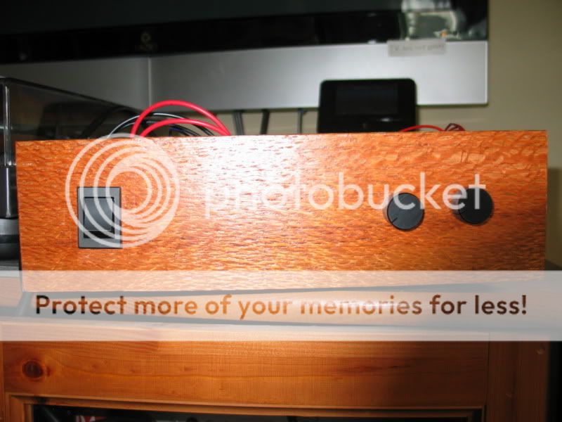
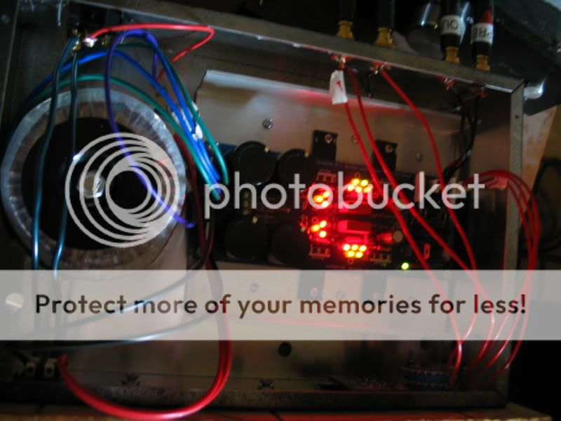
I finally got things installed into a Hammond case and the front panel is Lacewood.
I have had this DCB1 board in my desk drawer for at least six months, I was so content with my Pass diy B1 with TX2575 and Sonicaps w/teflon bypass that i just didnt have any incentive.
I am SO glad I took the plundge, this thing rocks and eaisly dethrones my current B1. As been said before the soundstage is scary big, low level detail is off the charts. I am listening at much lower levels with all the detail and resolution.
Build list includes:
Mundorf AG caps
TX2575 220r
Caddock 132 1m
Caddock TF020 220k
Antek 100va
Another big thanks to Salas,Teabag,Blues and Ed.
- Home
- Source & Line
- Analog Line Level
- Salas hotrodded blue DCB1 build