If you have a hard time understanding the circuit.... Imagine that you remove the GROUND pin from where it is, to the middle point between the capacitors ... then you will have a classic common-emitter (CFP/Sziklai) output stage.
Basivcally it is just a matter of wether you use the positive or negative speaker termeinal as power-ground.
Basivcally it is just a matter of wether you use the positive or negative speaker termeinal as power-ground.
First time i have adopted this circuit i thought about it as "complementary circlotron circuit", that's like circlotron for complementary devices or as "parallel circlotron" vs. normal "series circlotron"
Francesco,
in your schematic you don't have a connection from the speaker-connection between the two big caps to the center tap of the transformer, but the QSC-circuit has. Does that make a difference?
in your schematic you don't have a connection from the speaker-connection between the two big caps to the center tap of the transformer, but the QSC-circuit has. Does that make a difference?
Francesco,
in your schematic you don't have a connection from the speaker-connection between the two big caps to the center tap of the transformer, but the QSC-circuit has. Does that make a difference?
Yes, my choice is for a better separation between the power supply capacitor's charge current and the output stage audio current: the first mainly among the 5000microF, the last across the two 10.000 microF caps.
this schematic incorporates the "classic" mistake of combining the PSU charging circuit with the Audio output circuit.
The charging pulses feeding C510 & C511 must not share any common trace nor wire with the Audio side of the amplifier. They must be separated. Then connect from PSU zero/common Volts to the Main Audio Ground.
Look carefully at the length of wire connecting C510 to C511. Study it. It shows exactly what must NOT be done.
Agreed, although I think the schematic is representative of the logical rather than the physical connection of the caps. Any designer worth their salt will put the connection of the PSU charging circuit and the amp power supply at the actual capacitor pin. A more experienced one may put two caps in parallel, and connect the charge circuit to the first, and the amp power supply to the second.
As for the 'inverted' circuit itself, it's really a logical equivalent of the standard circuit with the parts mixed up a bit. That being said, it's NOT equivalent to the circlotron. The circlotron uses completely floating power supplies and notionally (usually not literally) grounds the center of the load, making each output half unity coupled - it's a follower and a common emitter/source at once with half of the load on each side. How the actual load appears impedance-wise, depends on the class of operation.Also, both halves use the same polarity amplification device, be that a tube or transistor of any species. The Sumo Nine is such an amplifier.
Hafler, QSC and member's mos57 VFET amp use 'AC' coupling in the output, where the PSU filter caps also serve as output coupling caps. Not so long ago there was a long discussion on the influence of PSU caps, where it was stated that most of the time PSU caps ARE coupling caps, and to an extent, this is correct. However, in this sort of circuit, they are ALWAYS coupling caps and although the circuit looks fine in theory, in the real world it's not without problems.
For one thing, any difference of capacitance between the two caps in series translates to a DC offset of the midpoint since the caps form a capacitive divider. Also, the ripple on the 'rails' is not equal. Because the amp is basically capacitively coupled, and the NFB is then taken from behind the cap, it has to behave differently for DC or it will want to 'lean' towards one output rail reducing headroom (simplest way to fix it is using substantial bleeder resistors across the caps to equalize the voltages on them, and properly dimension the DC blocking cap in the NFB loop). The unequal ripple gives the NFB a bit more to do which may increase intermodulation products with multiples of the mains freqency, but in general it's not much more than an equivalent amp of classical construction. As for no need for a DC protection circuit, this is a very moot point as then the caps need to be able to withstand the whole rail-to-rail voltage, rather than half of that when a center tap is provided on the transformer. Caps are not cheap, so it's quite probable that a DC protect sircuit and center tap on the transformer cost less.
For one thing, any difference of capacitance between the two caps in series translates to a DC offset of the midpoint since the caps form a capacitive divider.
Is this also the case if the cap's mid-point is connected to the trafo's center tap? This should assure that the voltages are equal, shouldn't it?
"Is this also the case if the cap's mid-point is connected to the trafo's center tap? This should assure that the voltages are equal, shouldn't it? "
The assertion that:
"Hafler, QSC and member's mos57 VFET amp use 'AC' coupling in the output, where the PSU filter caps also serve as output coupling caps. "
Is not entirely correct, many QSC have the output taken from the center tap of the transformer.
http://qscaudio.com/support/library/schems/Discontinued/MX%20Series/MX1500.pdf
http://qscaudio.com/support/library/schems/Current/RMX%20Series/RMX2450.pdf
Here is a Hafler with the output connected to the center tap:
IMAGE
Last edited:
As for the 'inverted' circuit itself, it's really a logical equivalent of the standard circuit with the parts mixed up a bit. That being said, it's NOT equivalent to the circlotron. The circlotron uses completely floating power supplies and notionally (usually not literally) grounds the center of the load, making each output half unity coupled - it's a follower and a common emitter/source at once with half of the load on each side. How the actual load appears impedance-wise, depends on the class of operation.
This is incorrect, now. In 2005 I have patented a circlotron with voltage gain, and then on this forum there is a thread about "the amazing fet circlotron" by M. Rothacher that also have voltage gain; in this cases i see similarity of the two circuits as i have explained above.
Okay, can someone please tell me what I did here? 😱
I built a simple CFP output stage and stepped a voltage source which represents the bias voltage. Then I plotted the currents through the emitter resistors to see the quiescent current. Works quite ok for the normal circuit. Then I "switched" the ground from one side of the load to the other. Look what that did to the current distribution between the two halves! What happened?
I tried do adapt several output stage types to the "inverted" configuration, but did not manage to find something that looks like it could be usefully biased. From what Enzo pointed out above, I thought I could simply switch the ground as I did here and everything should be fine, but it seems to me that this cannot be true...
Attachments
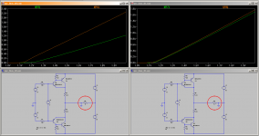
There is nothing wrong with the circuit, switching the ground around also means your circuit has changed from common collector to common emitter (*), i.e. it now has gain > 1 which also means the current gain difference between the halves is now blatantly visible.
In the right circuit, the difference between Vbe versus Ic (*) of the top and bottom parts is only transfered to the output, because the circuit is a follower. Because of the exponential nature of the Vbe vs Ic relationship, the resulting offset on the output is very small, on the order of millivolts - this small voltage only creates very small currents through the load, and most of the current passes from the top to the bottom half - hence very close spaced lines for the current of the top and bottom half, and almost perfect current distribution.
The left circuit, however, has voltage gain. Now the difference in Vbe versus Ic of the top and bottom part is not merely merely transferred to the output as as small offset voltage, it is also signifficantly amplified, producing a signifficant voltage on the load, causing part of the current to flow through the load, and this current is the difference between the current graphs for the top and bottom side. To verify this, plot voltage on the load alongside the current graphs for both cases.
(*) keep in mind that a CFP in fact looks like an augmented first transistor in the pair, so even though the second transistor works in CE, the whole pair looks like a larger transistor working in CC, that's what I mean when I say the configuration has changed from common collector (i.e. follower) to common emitter. Your circuit on the left is not a follower, it would only be one if you also changed the reference of the input side, to the center of the power supply.
Last edited:
Okay, this took me some time to understand. Seems like I'm lacking some of the basics 😱.
If I got you right, the regular CFP is a common collector augmented by a common emitter, acting as a CC. If I switch the ground now, I don't have a CC anymore but a CE. Looking at the schematic above, I see a CE augmented by a CC, which is very similar to the "switched CFP". Please correct me if I'm wrong here 🙂. Is this topology comparable to the regular CFP? Does it have the same thermal behaviour, for instance? Am I right in assuming that I do need a CE output stage for the usual biasing methods to work correctly in this case?
I'm having a hard time with my simulations, since I can only use a trial-and-error approach, which is kind of frustrating... 🙁
This is not at all that complicated. They called the other terminal of the speaker "ground" and that it's all. The rest of the amplifier has a different ground, which is the bad part of this.
Completars with colectors tied together have been used since 1980's.
Completars with colectors tied together have been used since 1980's.
They called the other terminal of the speaker "ground" and that it's all. The rest of the amplifier has a different ground, which is the bad part of this.
That would not make much sense. In the QSC circuit the input ground and speaker ground are connected trough a 3.3 Ohm resistor, which is quite common in "regular" amplifiers, too. The whole point of this circuit is that the power transistors can be mounted to the heat sink w/out insulators and the sink is mounted to the (grounded or "earthed") case. That would not be possible if you simply called the amp output "ground".
- Status
- Not open for further replies.
- Home
- Amplifiers
- Solid State
- "Inverted" (not 'Inverting') Output Stage