Take into account that the max permissible difference between remote clock and local clock can be ~200ppm (a tent clock has +-100ppm).That 4k won't last more than a few milisec.
This means that for 12.288MHz 200ppm is only 2457.6Hz. Channel data comes in serial, with a minor glue logic we can make it parallel before the buffer so half 2457.6Hz would be 1228.8Hz samples per sec. Thus a 4K buffer would be enough for ~3.3sec. Of course we want this difference much smaller, maybe 10-20ppm don't thought about this, thus 4K will buffer 20-30secs of data.
I don't like math...
Last edited:
I'm already planning to do this myself, and the whole CPU system is well under the price of that single FIFO. Well under meaning less than half. Why bother with Atmel or PIC when you can have the real thing - ARM?
Why spend money on hardware when software implementation is that much cheaper and fewer chips too? The ARM solution also gives flexibility for adding cool stuff like volume control, or filters... 😀
Why spend money on hardware when software implementation is that much cheaper and fewer chips too? The ARM solution also gives flexibility for adding cool stuff like volume control, or filters... 😀
I'm a developer, software can be buggy. Plus I like much more to solder smd parts then debug code 🙂
Sure, software can be buggy. So how are you going to program Atmel and/or PIC without software? At least ARM has decent debugging features.
Let's agree that it can be done in both ways. I mentioned the hardware FIFO because my uC knowledge is very limited but enough (with some help) to do the controlling part, that's it.
Anyway, everybody thinks that this FIFO path is a good one?
Anyway, everybody thinks that this FIFO path is a good one?
Last edited:
Well I already accepted your method is a possible method but its way suboptimal. If you want to sell it (and who doesn't want to earn some pocket money?) then you'll be severely undercut. ARM in digital audio is the future - so why not teach yourself and expand your business options? I'm starting my own training business using ARM, there's huge opportunity to get in right at the start. If you stick with PIC and Atmel you'll miss the boat 😛
<edit> No, that FIFO will work but its not 'good' in this application by any stretch of the word 'good'
<another edit> To get you started, I reckon NXP LPC1763 could be a great part for this. Its about $5 and includes 64k SRAM. On second thoughts, LPC1758 might be even better.
<edit> No, that FIFO will work but its not 'good' in this application by any stretch of the word 'good'
<another edit> To get you started, I reckon NXP LPC1763 could be a great part for this. Its about $5 and includes 64k SRAM. On second thoughts, LPC1758 might be even better.
Last edited:
I asked whether this FIFO buffer concept might be a good solution to deal with jitter or not. Didn't asked for a specific implementation<edit> No, that FIFO will work but its not 'good' in this application by any stretch of the word 'good'
(my English might need some polishing).
I'm curious, what else can be a bottleneck with this solution?
1. Peufeu mentioned the stability of the control voltage of the local VCXO
Last edited:
Yeah, the FIFO concept is part of the solution to deal with jitter. But only part - the control of the VCXO is the clever part that actually does the dejittering. That needs some software. I've considered this challenge at length and wonder whether fuzzy logic might be the best way to tackle it. Fuzzy logic control is used in quite a lot of consumer appliances nowadays.
Fuzzy logic is not necessary.Hardware FIFO is not necessary.uProcessor is not necessary.Big secret is not necessary. Don't you guys read your own forum?One true thing ThorstenL posted. SPDIF is dead. You know, like vinyl...
Hi,
That is one way of doing it. We use a different one.
Good summary.
Abbingdon Music Research - Products - Digital Processor-777
It would need a very fast CPU. We use a farily slow CPU instead and use the FIFO in the FPGA that also contains a lot of other stuff. We would have used a CPLD/FPGA anyway, we just used one a few sizes up.
The FPGA also holds some other key elements of the systems (the really "secret" ones)... The development of the Software for both was severely non-trivial.
Ciao T
OK, that makes it clearer.
I guess you use some kind of slow multibit DAC (SPI, I²C or otherwise) to vary the control voltage on a VCXO.
That is one way of doing it. We use a different one.
So your PLL which is not a PLL, would have an extremely low cutoff frequency, quantized frequency steps, and a very slow, intentionally limited frequency slew rate, so it doesn't try to track the source clock, but only very lazily adjust to keep the FIFO happy.
Good summary.
Hey, what product is that in ?
Abbingdon Music Research - Products - Digital Processor-777
As you're already using a uC, why wouldn't you have that CPU's memory do the job of the FIFO?
It would need a very fast CPU. We use a farily slow CPU instead and use the FIFO in the FPGA that also contains a lot of other stuff. We would have used a CPLD/FPGA anyway, we just used one a few sizes up.
The FPGA also holds some other key elements of the systems (the really "secret" ones)... The development of the Software for both was severely non-trivial.
Ciao T
It would need a very fast CPU. We use a farily slow CPU instead and use the FIFO in the FPGA that also contains a lot of other stuff. We would have used a CPLD/FPGA anyway, we just used one a few sizes up.
I'm betting your FPGA is faster than my CPU.😀 But sure, a decently fast CPU is not a problem nowadays. 50MIPs under $2 all in. But more if you need more SRAM for your buffer, SRAM's more silicon hungry than an ARM CPU.
This is not true. Apply the same concepts as your SD Card Player all across, but use a FIFO and make sure you can precisely set the clock to match the source.
During the time both left and right samples are stable, there should be lowest possible interference (bleed trough) on sample amplitude. Compare the sample (during its steady state) as a DC voltage that needs to have lowest possible noise superimposed on it. Every single interference source in the system will contribute to increased noise levels on the sample. The jitter attenuation circuit itself also introduces interference (bleed through), so a jitter attenuation circuit that actually provides low jitter levels can still introduce unacceptable interference levels that bleed though and result in noise on the sample during its steady state.
This large bandwidth interference (bleed through) includes the audio spectrum. Then it is very difficult to attenuate (filter) this noise without affecting the audio signal.
Keeping sample noise levels down is equally important than keeping jitter levels down.
This means that the digital audio source requires both, lowest possible interference levels AND lowest possible jitter.
When using S/PDIF interface that is converted to I2S to drive the DAC chip, assuming jitter levels and spectrum are identical for both. You will have interference (bleed through) from both, SPDIF signal and I2S signal. In direct I2S systems (no signal conversion to S/PDIF) this interference is completely eliminated and there will be zero S/PDIF bleed through. This is one of the advantages NOT using S/PDIF.
I2S however also has its flaws, as it also generates interference (serial data transfer during sample steady state). The best solution would probably be a DAC chip with parallel interface, enabling latching the data into the DAC chip during sample change and provide very low interference (since nothing gets clocked-in) in the sample steady state. This however would require 32 I/O lines plus latch for 16 bits and 48 I/O lines plus latch for 24 bits. This approach has the aim of reducing the interference levels on the DAC chip during sample steady state.
Then it does not matter if we fill the FIFO from a hard drive, a CD Drive, an S/PDIF Receiver, a USB device or even a thumb-drive. All of them are given "True Memory Playback" and locked only to your clock.
I had this illusion some years ago. Turned out I didn't realize the impact of source and interlink interference bleed through.
When striving for ultimate performance digital audio playback systems, jitter amplitude should be reduced to lowest possible value, the jitter spectrum of the remaining jitter should be as neutral as possible. Similar the interference levels on the sample during steady state should be as low as possible and the remaining noise should be white noise.
With these things in mind, there are clear differences between various digital audio sources, interlinks and jitter attenuation concepts. This will then result in a typical "digital fingerprint" for each concept.
I had this illusion some years ago. Turned out I didn't realize the impact of source and interlink interference bleed through.
+1E9. You're talking my language - CM noise by any other name.
Hi,
Noise (e.g. through supply lines, or ground contamination) is another issue, however, I think you still fail to understand the operating principle. There is no "jitter attenuation circuit".
In my solution there is a Memory Chip that contains audio samples, which are read out by a local clock. This is the precisely same structure as with your SD card player.
The fact that the memory is filled with data from an SPDIF receiver or a USB source is incidental and need not concern us, if we have implemented that part correctly (isolation, layout etc.).
SPDIF bleed-trough assumes a path for the SPDIF signal to reach the clock and/or other circuitry. It cannot do so via the signal lines, leaving PSU and Grounds. Now dealing with these is trivial in principle (just use enough separate power sources and block RF bleed through from one into the others).
Really, this part is quite simple.
This we actually both agree upon, but I2S or EIJA serial interfaces is what we have.
You never attempted anything like the solution I have applied. I am aware of your attempts to reduce jitter, these can work to a degree, but they are not very effective at all.
My solution delivers this.
This is a function of the other areas in the design. BTW, I dislike white noise like jitter, I strongly prefer "pink" noise for what remains.
Of course. The problem is that "jitter attenuation" only reduces jitter amplitude. One needs "jitter removal" to eliminate source jitter.
Sadly all digital sources radiate all sorts of RFI noise, which tend to effect other parts of the systems and so even if all else is exactly equal two different sources may still produce different sound quality, however to blame the DAC (be it for common mode noise or jitter) in this case may seem obvious, but does not always hold true.
Ciao T
During the time both left and right samples are stable, there should be lowest possible interference (bleed trough) on sample amplitude. Compare the sample (during its steady state) as a DC voltage that needs to have lowest possible noise superimposed on it. Every single interference source in the system will contribute to increased noise levels on the sample. The jitter attenuation circuit itself also introduces interference (bleed through), so a jitter attenuation circuit that actually provides low jitter levels can still introduce unacceptable interference levels that bleed though and result in noise on the sample during its steady state.
Noise (e.g. through supply lines, or ground contamination) is another issue, however, I think you still fail to understand the operating principle. There is no "jitter attenuation circuit".
In my solution there is a Memory Chip that contains audio samples, which are read out by a local clock. This is the precisely same structure as with your SD card player.
The fact that the memory is filled with data from an SPDIF receiver or a USB source is incidental and need not concern us, if we have implemented that part correctly (isolation, layout etc.).
When using S/PDIF interface that is converted to I2S to drive the DAC chip, assuming jitter levels and spectrum are identical for both. You will have interference (bleed through) from both, SPDIF signal and I2S signal. In direct I2S systems (no signal conversion to S/PDIF) this interference is completely eliminated and there will be zero S/PDIF bleed through. This is one of the advantages NOT usin S/PDIF.
SPDIF bleed-trough assumes a path for the SPDIF signal to reach the clock and/or other circuitry. It cannot do so via the signal lines, leaving PSU and Grounds. Now dealing with these is trivial in principle (just use enough separate power sources and block RF bleed through from one into the others).
Really, this part is quite simple.
I2S however also has its flaws, as it also generates interference (serial data transfer during sample steady state). The best solution would probably be a DAC chip with parallel interface, enabling latching the data into the DAC chip during sample change and provide very low interference (since nothing gets clocked-in) in the sample steady state.
This we actually both agree upon, but I2S or EIJA serial interfaces is what we have.
I had this illusion some years ago. Turned out I didn't realize the impact of source and interlink interference bleed through.
You never attempted anything like the solution I have applied. I am aware of your attempts to reduce jitter, these can work to a degree, but they are not very effective at all.
When striving for ultimate performance digital audio playback systems, jitter amplitude should be reduced to lowest possible value, the jitter spectrum of the remaining jitter should be as neutral as possible.
My solution delivers this.
Similar the interference levels on the sample during steady state should be as low as possible and the remaining noise should be white noise.
This is a function of the other areas in the design. BTW, I dislike white noise like jitter, I strongly prefer "pink" noise for what remains.
With these things in mind, there are clear differences between various digital audio sources, interlinks and jitter attenuation concepts. This will then result in a typical "digital fingerprint" for each concept.
Of course. The problem is that "jitter attenuation" only reduces jitter amplitude. One needs "jitter removal" to eliminate source jitter.
Sadly all digital sources radiate all sorts of RFI noise, which tend to effect other parts of the systems and so even if all else is exactly equal two different sources may still produce different sound quality, however to blame the DAC (be it for common mode noise or jitter) in this case may seem obvious, but does not always hold true.
Ciao T
Impressive product !
Yeah, the very large number of frequency steps you mention doesn't really point to a DAC+VCXO... Are you using some form of DDS ?
> During the time both left and right samples are stable
This only happens with a multibit DAC, not with sigma delta DACs.
That is one way of doing it. We use a different one.
Yeah, the very large number of frequency steps you mention doesn't really point to a DAC+VCXO... Are you using some form of DDS ?
> During the time both left and right samples are stable
This only happens with a multibit DAC, not with sigma delta DACs.
Hi,
Thank you. We do try. I must say that using a tube as SPDIF input stage is a little whimsical and "because we can", but works quite well. Signals the normal SPDIF inputs cannot lock onto work fine with the extra circuirtry.
It is a specific programmable oscillator, one with low audio band jitter...
Quel Dommange - we have one of each...!
😀
Actually, after we had killed all the jitter from the source, we suddenly started seeing all sorts of jitter effects. Having the second (unused) DAC running in parallel with the main one increases jitter. Just having some activity on the I2C bus for the 32 Bit DS DAC does.
Ciao T
Impressive product !
Thank you. We do try. I must say that using a tube as SPDIF input stage is a little whimsical and "because we can", but works quite well. Signals the normal SPDIF inputs cannot lock onto work fine with the extra circuirtry.
Yeah, the very large number of frequency steps you mention doesn't really point to a DAC+VCXO... Are you using some form of DDS ?
It is a specific programmable oscillator, one with low audio band jitter...
This only happens with a multibit DAC, not with sigma delta DACs.
Quel Dommange - we have one of each...!
😀
Actually, after we had killed all the jitter from the source, we suddenly started seeing all sorts of jitter effects. Having the second (unused) DAC running in parallel with the main one increases jitter. Just having some activity on the I2C bus for the 32 Bit DS DAC does.
Ciao T
Are you using some form of DDS ?
I'm hoping that use of DDS is still blasphemy in high end audio. That's one of my potential market opportunities 😉
You never attempted anything like the solution I have applied
Well eh, I designed something that may be similar in 2008. I called it a frequency tracker. It uses a microcontroller (Microchip) to measure the exact frequency difference between source and masterclock (using on-chip hardware timers). The difference is loaded into a 10 bit discrete R2R DAC using parallel 10-bit interface in order to minimize noise levels. This DAC in turn drives the VCXO through a low pass filter.
The processor runs on the masterclock, avoiding inter-modulation and enabling smart frequency comparison (as the processor clock is one of both frequencies that need to be compared).
Masterclock frequency could be changed in approx. 1ppm steps, after correction, the masterclock remained fixed at that specific frequency. The correction interval was set to 2 seconds, but could also be extended.
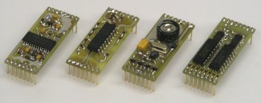
It's all well documented on my thread. I added a photograph showing S/PDIF receiver module (left), followed by frequency tracker, VCXO, and an interpolator module on the right that is not relevant here. I used it to connect to iMac plus iTunes (mini Toslink), Apple Airport express (Mini Toslink), and CD / DVD players (Toslink / Coax).
Attachments
Hi,
May be, but maybe not.
Not actually, if you ask me.
Ciao T
Well eh, I designed something that may be similar in 2008.
May be, but maybe not.
Not actually, if you ask me.
Ciao T
- Status
- Not open for further replies.
- Home
- Source & Line
- Digital Source
- Jitter? Non Issue or have we just given in?