Update:
I tried a new higher power toroid and that made no difference.
I tried an IRFB4227 pair driving my old 16 amp toroid and the amplifier now no longer resets even into hard clipping.
Just need to try another couple of pcbs with irfb4227 to ensure the fix is reliable, got some 4227's on order.
For some reason the irfb4019's (even four off) just werent man enough for the 500 watts I was trying for.
Someone once said "If something works first time you learn nothing, if it takes a lot of work to get going you have learned a lot"
The current working class d amplifier.
Larger inductor and more powerful output transistors than original layout.
Larger inductor and more powerful output transistors than original layout.
An externally hosted image should be here but it was not working when we last tested it.
Cold IRFB4019 can do 6A or so without body diode conduction.
Cold IRFB4227 can output 20A peak without substantial body diode conduction. They can do another 20A through the body diode with proper PCB and parasitics under control.
Poor layouts benefit from "heavy" MOSFET as a drop-in replacement because switching becomes much slower.
With same gate resistors and everything, IRFB4227 switches 4-5 times slower than IRFB4019.
Your circuit could work with IRFB4019 at full switching speed, but it would require moving things on the PCB, adding SMD decoupling caps and RC snubbers to the switching node and sometimes from gate to source.
Two obvious things you don't seem to have tried are reducing gate supply voltage (this controls turn-on di/dt current slope directly, which is directly related to EMI production). Increasing gate turn-on resistors has a similar effect but the mechanism is not exactly the same. Gate turn-off diodes in parallel with turn-on resistor are recommended.
The amplifier will start malfunctioning above a certain EMI level.
Thru-hole parts and long PCB tracks without ground plane will pick up all hash radiated by high di/dt in power traces with neither ground plane nor an "easy" return path.
Last edited:
Cold IRFB4227 can output 20A peak without substantial body diode conduction. They can do another 20A through the body diode with proper PCB and parasitics under control.
An irfb4019 has 80mohms RDSon and so should pass 16 amps before overcurrent protect jumps in. Two pairs as my original design should pass 32 amps. Neither way stopped the resetting.
The irfb4227 has about 18mohms RDSon and I used one pair and this means there is 72amps passing through the inductor !
Clearly I have missed something somewhere.
At worst case my 500 watt amp should take about 12 amps into the speaker.
Add to that losses in the output inductor/capacitor filter.
The overshoot and ringing is now considerably better with the 4227 mosfets.
An externally hosted image should be here but it was not working when we last tested it.
Last edited:
It's EMI what is tripping directly or indirectly the protection. It's not current itself, but high frequency voltage drops across PCB tracks proportional to track inductance and current slope (di/dt) that you are not accounting for and that spoil any voltage sensing above a few Mhz. There are many things happening in the circuit that you are not yet able to imagine.
IRFB4227 also has much lower capacitances, which translates into lower frequency ringing ( Fres=1/(2*pi*sqr(L*C)) ) which propagates less to adjacent tracks. This makes things easier (maybe at the expense of higher idle losses).
PCB tracks in close proximity with no ground plane are like well coupled inductors at RF.
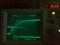
These are reference IRFB4227 waveforms at 500w and 1500W @ 4 ohm. It shows what optimum snubbers applied at the gate (tuned RCD), the switching node (tuned RLC) and the supply rails (big electrolytics, plus array of films as tuned RLC, plus one SMD C very close to each MOSFET) can do.
The amount of ringing you show is completely unacceptable.
Only class D amplifiers with clean waveforms can sound "clean".
IRFB4227 also has much lower capacitances, which translates into lower frequency ringing ( Fres=1/(2*pi*sqr(L*C)) ) which propagates less to adjacent tracks. This makes things easier (maybe at the expense of higher idle losses).
PCB tracks in close proximity with no ground plane are like well coupled inductors at RF.
These are reference IRFB4227 waveforms at 500w and 1500W @ 4 ohm. It shows what optimum snubbers applied at the gate (tuned RCD), the switching node (tuned RLC) and the supply rails (big electrolytics, plus array of films as tuned RLC, plus one SMD C very close to each MOSFET) can do.
The amount of ringing you show is completely unacceptable.
Only class D amplifiers with clean waveforms can sound "clean".
Attachments
IRFB4227 also has much lower capacitances, which translates into lower frequency ringing ( Fres=1/(2*pi*sqr(L*C)) )
That equation though translates lower C into higher frequency as its in the denominator.

Oh lord, that is horrible switching, even by my standardsAn irfb4019 has 80mohms RDSon and so should pass 16 amps before overcurrent protect jumps in. Two pairs as my original design should pass 32 amps. Neither way stopped the resetting.
The irfb4227 has about 18mohms RDSon and I used one pair and this means there is 72amps passing through the inductor !
Clearly I have missed something somewhere.
At worst case my 500 watt amp should take about 12 amps into the speaker.
Add to that losses in the output inductor/capacitor filter.
The overshoot and ringing is now considerably better with the 4227 mosfets.
An externally hosted image should be here but it was not working when we last tested it.
Looking at PCB, even if non smt used, board could be half the size, that being said, it is due to pcb layout that you are getting this, and missing key elements in key positions.
PCB is more then 80% of the designs, eva has proven to me a long time a go, that even with bad elements, and by bad, I mean really bad, 20y old elements, you can do a lot, if you measure, simulate and understand what is going on... give her some new and good stuff and god knows what will come out
you will need to redo the pcb, 2 sided is only way + ground planes, very important
I will try to look at my waveform today
That equation though translates lower C into higher frequency as its in the denominator.
Sorry, I meant 4-6 times higher capacitances.
you will need to redo the pcb, 2 sided is only way + ground planes, very important
I will try to look at my waveform today
The pcb is already 2 sided with very little room for a ground plane.
The pcb certainly cant be half the size without compromising track widths for the power.
Reducing the ringing does seem to improve matters.
I had one pcb with 12 volt ringing and another with 25 volts ringing and the first one worked almost perfectly. The second would reset around clipping level on the output.
I really cant be far away now !
Did a little more work tonight.
Just for interest I disconnected the speaker and the 2092 still resets on hard clipping.
Interesting it does that with no load.
I made both over current protects the max voltage they will go and there was no improvement in onset of resetting point.
Just for interest I disconnected the speaker and the 2092 still resets on hard clipping.
Interesting it does that with no load.
I made both over current protects the max voltage they will go and there was no improvement in onset of resetting point.
Cold IRFB4019 can do 6A or so without body diode conduction.
Have you tried hard clipping your amps to see how they behave ?
There is a note about being careful that VB doesnt drop too low or the 2092 will reset. Perhaps that is what I am getting now ?
I really took as much care as I could over the pcb layout but there is simply no room for getting things closer with the current track widthes. The power and ground tracks are as thick as possible.
I have tried extra decoupling and it makes no difference, just keeps resetting around the clipping point.
Interesting it does that with no load.
The problem is not the load, it's the layout.
I really took as much care as I could over the pcb layout but there is simply no room for getting things closer with the current track widthes. The power and ground tracks are as thick as possible.
I have tried extra decoupling and it makes no difference
No you didn't, yes there is, no they aren't, yes it does (if you do it right).
I've got three amps from classDaudio that do not exhibit your problem . . . perhaps you should drop a hundred quid on one of their boards and see how they do it . . .
Class D Audio Class D Audio Amplifiers - PRODUCTS
The problem is not the load, it's the layout.
I've got three amps from classDaudio that do not exhibit your problem . . . perhaps you should drop a hundred quid on one of their boards and see how they do it . . .
Class D Audio Class D Audio Amplifiers - PRODUCTS[/url]
I can manage a couple of hundred watts too even with my limited experience.
My amplifier is 500watts and thats about where the problems start.
Its not like I cant get a sound out of it or it can only manage a few watts.
Clearly I am well down the road but just cant quite reach the finishing post.
of course pcb can be half the size, also for this amp, you don't need 2 sided pcb only for tracks
I have all the tracks on one side, ground planes on other, and pcb is 10cm x 8cm
PCB size will be only as small as your components are, tracks are not a problem...
I don't konw if I have 4" of tracks from + to -, going through fets
I can't even imagine that I would use smt and smaller fets
I have all the tracks on one side, ground planes on other, and pcb is 10cm x 8cm
PCB size will be only as small as your components are, tracks are not a problem...
I don't konw if I have 4" of tracks from + to -, going through fets
I can't even imagine that I would use smt and smaller fets
In order to make that amp work you will need to ensure the following:
- 2 sided pcb with ground planes refered to input gnd, - and output gnd
- short traces from chip to the gates of the mosfets, from switching node to the output inductor, from + and - electrolytic caps to the mosfets
- good decoupling from + to gnd, - to gnd, drain of the upper mosfet to gnd, source of the lower mosfet to gnd, a 1uf cap from upper mosfet drain to lower mosfet source(as close as possible to the pins of the mosfets), vcc, vss, vaa decoupled with low esr electrolytic (or tantalum) caps paralleled with x7r smd caps.
- bootstrap cap has to be low esr paralleled by 1uf x7r smd cap
- 1% tolerance resistors
- rc snubbing on the mosfets tuned to tame ringing under 100mhz if possible
- nr 2 micrometals toroid core for output inductor or gaped ferrite RM series
- if possible separate power supply for vcc,vss and vaa to keep voltages steady while the power stage sags the main +/- supply due to high power bursts.
Regards,
Savu
Last edited:
no, that would be 3 grounds, one is power which is the same as input, which is the second
3rd is referenced to - supply, over fets and some of the IR pins (output gate drive, current sense)
You don't need 1% resistors, you can use normal 5%
While you could seperate supply, that is not needed
If you would use RM series core, what size core/material should one use and what gap for say 400-500w as this IC should do?
You could use something similar to bender.ru cakeamp for example of calculation.If you would use RM series core, what size core/material should one use and what gap for say 400-500w as this IC should do?
1% tolerance resistors should be indicated also low esr caps. It all depends on what you expect of the amp.
In total there are 2 electrical ground planes (GND and -). i fill the top side (component side) with one groundplane referenced to GND and the bottom side with 3 grund planes 2 referenced to GND and one to -.
Attachments
Update:
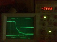
Noticed tonight that with a heavy load the inductor ringing gets much worse.
This is probably what is triggering the OCP reset.
Waiting for a T106-2 inductor to see if that improves matters, could be a while as it is coming from the USA CA.
In the meantime I am working on the next pcb with a ground plane.
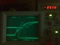
Managed to improve the switching waveform tonight.
Gone from 25volts of overshoot and ringing to 5 volts.
Will check it out on full power in the morning as I dont think the neighbours would appreciate now at 4am !
Scope is 10v/div.
Gone from 25volts of overshoot and ringing to 5 volts.
Will check it out on full power in the morning as I dont think the neighbours would appreciate now at 4am !
Scope is 10v/div.
An externally hosted image should be here but it was not working when we last tested it.
Last edited:
- Status
- This old topic is closed. If you want to reopen this topic, contact a moderator using the "Report Post" button.
- Home
- Amplifiers
- Class D
- irs2092 resetting with low frequencies.