Most (probably 100 %) Darlingtons are emitter followers.
CFP has lower distortion than EF.
hmm I dont know english names for all connection posibilities.
CFP ?
compare SOA @ 40Vce and 60Vce.1943 is 225 V 15A bjt with 150W dissipation ....
why if we take that current performance is good, why for dissiaption 75W (150W amplifier) would require SO much paralell bjt, you say 4 pairs, is not that too much ?
Now de-rate these SOA to take account of operating temperature.
You will find that a 3pair on a very big heatsink might just about have the same current capability @ 60Vce that a single pair on a medium heatsink will have at 40Vce.
This assumes that Re and Vre are similar for the two set ups.
hmm I dont know english names for all connection posibilities.
CFP ?
CFP: complementary feedback pair.
This link Semiconductor Safe Operating Area gives you valuable information regarding BJT SOA.
compare SOA @ 40Vce and 60Vce.
Now de-rate these SOA to take account of operating temperature.
You will find that a 3pair on a very big heatsink might just about have the same current capability @ 60Vce that a single pair on a medium heatsink will have at 40Vce.
This assumes that Re and Vre are similar for the two set ups.
Lets consider just single pair..
Lets say we have 100W amplifier with single pair output. Lets say its pure class B which has maximum dissipation at 40% of maximum output power. So maximum disspiation is 40W (ideal amplifier not real) if both transistors are indentical in that pair than its just 20W of dissipation per single transistor. All in all in class B when there is maximum voltage Vce than current is minimal... so how can this go outside SOA ?
In the worst case lets say that 100W amplifier dissipates 100W of power. or 50%. Thats 50W per bjt.
EDIT. I see now sound.wst link.. so I will look that later.. Seems that speaks has great current to voltage angle(not in phase).. so current on bjt may be great..
Last edited:
CFP: complementary feedback pair.
This link Semiconductor Safe Operating Area gives you valuable information regarding BJT SOA.
this sound wst. calculation about soa seems completely weird.
If we put bjt with cooler in the room where is ambient air temperature 150 C than dissipation will be 0W, because any currnt throught bjt will rise it over 150 C.
this same bjt mounted on this same cooler may be inside room where is 25C and junction can be at 150C. Lets say that cooler aluminum as at 130C (because thermal reistance from junction to cooler) than at this point according to thermal resistance of cooler dissipation may be significant in Wats.
.
otherwise it does not make sense hmm, ot I may be wrong 😀
Seems that this graph http://sound.westhost.com/soa-f2-1.png
than shows us thermal resistance from junstion to case. Because if we have all thermal resistances we should easly calculate maximum dissipation.
The is derating curve of a 230 W transistor.
What can make the heatsink 130 C? It can be the transistor handling high power. The heatsink is too small which has a very high thermal resistance from heatsink to air. High thermal resistance from junction/case to heatsink make the junction/case hot, not the heatsink. A big big heatsink can be cool but the transistor case/junction is very hot due to poor contact (high thermal resistance from case to heatsink).
What can make the heatsink 130 C? It can be the transistor handling high power. The heatsink is too small which has a very high thermal resistance from heatsink to air. High thermal resistance from junction/case to heatsink make the junction/case hot, not the heatsink. A big big heatsink can be cool but the transistor case/junction is very hot due to poor contact (high thermal resistance from case to heatsink).
The is derating curve of a 230 W transistor.
What can make the heatsink 130 C? It can be the transistor handling high power. The heatsink is too small which has a very high thermal resistance from heatsink to air. High thermal resistance from junction/case to heatsink make the junction/case hot, not the heatsink. A big big heatsink can be cool but the transistor case/junction is very hot due to poor contact (high thermal resistance from case to heatsink).
It was wrong translation by me .. Tc is temperature of BJT housing or bjt metal plate .. I thought that Tc means junction temperature ..
Than graph linked before is DIRECT consequece of thermal resistance between junction and housing...
In the datasheet stays : SOA graph values decrease linear: does it mean both for Vce and Ic ?
for example we have Tc 25C and 10A Ic and 10V Vce limit(just example not direct graph)... for 50 C what would be SOA values ?
a1943/c5200
just compare Ic @ 40Vce and 60Vce to get some idea.
We can leave the temperature de-rating for the next part of the discussion.
~3.75A vs ~1.4A
just compare Ic @ 40Vce and 60Vce to get some idea.
We can leave the temperature de-rating for the next part of the discussion.
~3.75A vs ~1.4A
Last edited:
just compare Ic @ 40Vce and 60Vce to get some idea.
We can leave the temperature de-rating for the next part of the discussion.
~3.75A vs ~1.4A
Ok lets take 100W RMS amplifier -/40V(Vcemax) DC and 8ohm speaker.
2SA1943 : gives at 40V 3,75A lets say we have 50% eff and 100W dissipation.
WHAT is maximum degradation related to Tc possbile here ? SOA graph says that single BJT can dissipate 40*3,75=150W at Tc= 25 C
25C > 150W > 3,75A
than at 50C> 120W >40V>3A
at 150 C 0V 0A
Here 40Vce is maximum , not effective... and dissipation and SOA can only be claulaated to average voltage and average current
is this ok
Last edited:
you won't get 100W into 8r0 from +-40VdcOk lets take 100W RMS amplifier -/40V(Vcemax) DC and 8ohm speaker.
2SA1943 : gives at 40V 3,75A lets say we have 50% eff and 100W dissipation.
Rather than get complicated with temperature, just look at the current capability of the 1943/5200 at the two Vce. 40Vce for ~70W and 60Vce for ~160W
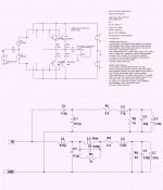
What are the value of R2/R3 and R5/R6? B-E of Q1/Q4 can be reversed bias for high voltage leading to breakdown.
The only time B-E can be reversed is when the OPT devices draw negative current. I don't see how that can happen as the emitter degeneration resistors can only go in the positive direction. For example, on the negative swing (outside of the A range), there is a drop across R4, but there is no drop across R1 because there is no current. R2/R5=220R R3/R6=4K, notice that R1/R4 are 0.22.

The only time B-E can be reversed is when the OPT devices draw negative current. I don't see how that can happen as the emitter degeneration resistors can only go in the positive direction. For example, on the negative swing (outside of the A range), there is a drop across R4, but there is no drop across R1 because there is no current. R2/R5=220R R3/R6=4K, notice that R1/R4 are 0.22.
Well, my question was the value of R3/6 and R1/4. Given your values, BE is not reversely biased. If, say, 4 k is replaced by 1 k, you will have a different picture.
The only part of the picture that would change when R3/R6 is changed from 4K to 1K is the slope of the loadline in the SOA graph. By creating more padding with a 1K the point where limiting takes place is higher and is now less sensitive. IOW, the current limit per device might be 2.12A per device under a shorted load, but the 2 Ohm limit might now be 5A instead of a more correct 2.6A
2r0 of load and what value of limited output current? It must be a lot more than 2.6Apk, maybe 20Apk or 30Apk?IOW, the current limit per device might be 2.12A per device under a shorted load, but the 2 Ohm limit might now be 5A instead of a more correct 2.6A
2r0 of load and what value of limited output current? It must be a lot more than 2.6Apk, maybe 20Apk or 30Apk?
Without the SOA limiter, you'll be around 9A per device. The magic smoke will depart soon.
V(n011) is the base of Q6. The emitter is V(out). It only goes positive
Did you try for Rload = 8 Ohms?
smoke from where?Without the SOA limiter, you'll be around 9A per device. The magic smoke will depart soon.
9Apk from a single device seems quite reasonable for a short term transient.
- Home
- Amplifiers
- Chip Amps
- LME49810 - a new cousin for LM4702