I've been looking around at different topologies trying to figure out as much as I can and I think I've figured out a few things, but I'd like to hear what you guys all think about it.
I've done some distortion searching using Doug's information and the ESP web pages.
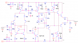
I changed up the standard input stage a bit and here's why/how...
Firstly,
I reduced the Current Mirror Emitter resistors because 94mV seems to be sufficient to account for changes in Vbe that I've seen while building my test amps. I think I might even try to go further down to 22R's for reasons I state below, if I think I can get away with it without any Vbe problems.
Secondly,
Also I added a current mirror buffer because if I assume that the transistors have a Beta of about 200. 2ma output requires 10ua of base current. Since one side has both bases on it, I can expect to loose 20ua from side to side. That gives me a 1% delta right off the start.
Using Doug's articles as a guideline, a 2% difference in current matching equates to an increase from .1% to .16%THD which is huge!😱 Using a single buffer, now the lost current equates to almost nothing. 20ua/200 = 100nA or .005% delta. That's gotta be close enough, right?
I've made an easy check on the VAS which I think is important.
Shown by Doug Self, Emitter resistance on the current mirror can bring out VAS distortion thus I thought it very important to keep Current Mirror Emitter resistors low and the size of Cdom Small (obviously). But also I think I have found my previous problem. I forgot to look at the VAS Transistor capacitance and its base resistor pull down.
I presume that the first amp I built with "Interesting" VAS transistors had it's problem with this value and I just didn't know what was happening.
Finally, the Driver Stage.
I know that typically there is a resistor/Capacitor between the drivers to cause the output base currents to evacuate more quickly and thus speedup turn off times. Using the capacitor just creates less impedance with increasing frequency, thus at some frequency, I assume it will cause IMD by shorting the output bases to each other thus eliminating the bias all together. Thus this seems like a band-aid rather than a fix, if you ask me.
However, I have recently seen the "Mongrel" amplifier which seems to have fixed this problem with a simple solution, CCS's on the output bases allows them to be shut off while not producing the zero impedance issues.
In my design I don't claim to even try to push enough current through the CCS's to bias the drivers into Class A, because I personally think that as long as they exist they will turn off the drivers as needed. Mainly they will push the drivers class B switch off point slightly away from 0V on the input signal, or to say it a different way, the drivers will be forced into class AB territory while the outputs can be biased independently.
I think this really buys you the fact that now your drivers and outputs don't have to be turned off simultaneously, the outputs will be turned off naturally on the way down using the CCS and the drivers will be left with the nasty/slower turn off effects. But since the drivers are now separated from the output signal it doesn't really matter does it? The question is really, just how much current do we need to ensure that those outputs get turned off effectively?
6ma has a slew limited frequency of 10mhz with my 600pf output drivers, maybe thats not high enough... I dunno. 1.2V bias and the 200R typ. resistor make about 6ma, that's my entire reason for choosing that value.
Any Comments on my Analysis or Circuit? I hope so!
I've done some distortion searching using Doug's information and the ESP web pages.
I changed up the standard input stage a bit and here's why/how...
Firstly,
I reduced the Current Mirror Emitter resistors because 94mV seems to be sufficient to account for changes in Vbe that I've seen while building my test amps. I think I might even try to go further down to 22R's for reasons I state below, if I think I can get away with it without any Vbe problems.
Secondly,
Also I added a current mirror buffer because if I assume that the transistors have a Beta of about 200. 2ma output requires 10ua of base current. Since one side has both bases on it, I can expect to loose 20ua from side to side. That gives me a 1% delta right off the start.
Using Doug's articles as a guideline, a 2% difference in current matching equates to an increase from .1% to .16%THD which is huge!😱 Using a single buffer, now the lost current equates to almost nothing. 20ua/200 = 100nA or .005% delta. That's gotta be close enough, right?
I've made an easy check on the VAS which I think is important.
Shown by Doug Self, Emitter resistance on the current mirror can bring out VAS distortion thus I thought it very important to keep Current Mirror Emitter resistors low and the size of Cdom Small (obviously). But also I think I have found my previous problem. I forgot to look at the VAS Transistor capacitance and its base resistor pull down.
I presume that the first amp I built with "Interesting" VAS transistors had it's problem with this value and I just didn't know what was happening.
Finally, the Driver Stage.
I know that typically there is a resistor/Capacitor between the drivers to cause the output base currents to evacuate more quickly and thus speedup turn off times. Using the capacitor just creates less impedance with increasing frequency, thus at some frequency, I assume it will cause IMD by shorting the output bases to each other thus eliminating the bias all together. Thus this seems like a band-aid rather than a fix, if you ask me.
However, I have recently seen the "Mongrel" amplifier which seems to have fixed this problem with a simple solution, CCS's on the output bases allows them to be shut off while not producing the zero impedance issues.
In my design I don't claim to even try to push enough current through the CCS's to bias the drivers into Class A, because I personally think that as long as they exist they will turn off the drivers as needed. Mainly they will push the drivers class B switch off point slightly away from 0V on the input signal, or to say it a different way, the drivers will be forced into class AB territory while the outputs can be biased independently.
I think this really buys you the fact that now your drivers and outputs don't have to be turned off simultaneously, the outputs will be turned off naturally on the way down using the CCS and the drivers will be left with the nasty/slower turn off effects. But since the drivers are now separated from the output signal it doesn't really matter does it? The question is really, just how much current do we need to ensure that those outputs get turned off effectively?
6ma has a slew limited frequency of 10mhz with my 600pf output drivers, maybe thats not high enough... I dunno. 1.2V bias and the 200R typ. resistor make about 6ma, that's my entire reason for choosing that value.
Any Comments on my Analysis or Circuit? I hope so!
Attachments
Last edited:
I thought that too for far too long.Also I added a current mirror buffer because if I assume that the transistors have a Beta of about 200. 2ma output requires 10ua of base current. Since one side has both bases on it, I can expect to loose 20ua from side to side. That gives me a 1% delta right off the start.
GK put me right.
It's down to setting up the VAS base current to exactly equal the sum of the mirror base currents.
Then the mirror is accurately balanced if the components are carefully matched as a full set, resistors, mirror transistors, VAS transistor.
The diamond arrangement driver is more usually used for small currents not as poweramp drivers.
What about looking for corroboration that either drivers be inserted between diamond and output devices or your chosen 6mA bias for drivers.
The extra resistor that D.Self uses is inserted into your Vbe multiplier. But the tapping to feed the drivers is taken from the wrong end of the extra resistor.
Last edited:
Think you have done a good job.
Looks very good.
Some minor points I notice:
A) The 10k resistor to the base of input.
It is too high value.
Try 1k or 2k2. This is more normal.
B) The cap 47uF across VBE-multiplier.
Think this is way to high value.
My simulations show 1uF or 2.2uF.
1 uF is commonly used as far as I have seen.
C) Input mirror at bottom.
The transistor in between works at only base currents.
Try one 1k-2k2 resistor from the emitter to V-
It is from the junction of the two bases and emitter of middle transistor.
I have tested this type of mirror in SPICE
and at several occations were lowest distortion with ~1.8k resistor.
Makes this transistor work at like 0.400 mA
Last edited:
Think you have done a good job.
B) The cap 47uF across VBE-multiplier.
Think this is way to high value.
My simulations show 1uF or 2.2uF.
1 uF is commonly used as far as I have seen.
Lineup if you do some stability plots with regards to the biasing circuit youll see why a higher value is actually better to ensure bias circuit stabilty, then have a look at some good, better than average commercial designs and see how their designers go it right. I wouldnt go below 10 uf and higher is better especially if youre using low esr type caps which have better sound quality.
Awesome input! I've made some changes.
The driver input on the wrong side of Vbe was just an error.
Maybe I'm just tired, but what is a "Diamond Arrangement Driver"? Did I draw one of those?
The pull down resistor on the current mirror seems to be in question, I can see where andrew is coming from because I briefly thought about the vas current. But I assumed (without checking) that the EF setup on the Vas would sink almost no current because of the ridiculous gain. Its gonna be on the order of 200^2.
Ok so I'm gonna try to go through it. I think that the steady state (No signal) is very close to when the VAS is pulling 6ma (the entire current source). Thus there is no current left for the drivers and the state of the the output is nominal, just bias alone. I hope I'm not being stupid here...
Now using a gain of 200 for the vas transistors I get a gain of 40,000 total from input to Vas output. For 6ma/40,000 = 150na. Which is awesome since the other side is loosing 100na to the buffer. Which means my offset is actually closer to 0 than I thought, but only by happenstance. 😀 I'm ok with that...
To make it academic, I need another 50ua from the current mirror, so lets try that resistor...
Using the idea for the resistor on the current mirror, lets see where we get. I need 150na from the base of the buffer to cancel the 150na going to the VAS, so that's 150na*200= 30ua at the common base. 20ua is being used by the transistors, so I need to shunt another 10ua to V-. Assuming .6V Vbe and the 94mV across the emitters I get .694V and thus to get 10ua I come up with 70k?
I like the idea of having a resistor there, if only for peace of mind that the buffer has a standing current no matter the state of the mirrors... But I cant get to the 2k number, Maybe I'm missing something that is just empirical?
As far as the 47uF Cap across the Bias, its specified in Doug's work and the Mongrel has a 10uF there, so I don't think I'm sooo off base. But to be honest I don't really know what its for...
I assume to keep the bias voltage constant? Wouldn't bigger be better for that use?
I get confused sometimes in the uses of capacitors, like this one. I know at 20khz its got almost no impedance, but... Ehh, my head hurts. 😕
Maybe I'm just tired, I'm going to sleep...
Thanks guys! Keep the bullets coming 😛
Attachments
Hi,
that 68k can be implemented with or without the third mirror transistor.
Forget about 200^2.
Look at the VAS and EF separately.
The VAS passes 6mA of Iq. Ic varies from an extreme of 0mA to ~2 to 3times Iq.
Lets say that is a range of 0 to 18mA.
Using hFE for that range of Ic, what is the range of base current and Ibquiescent?
Now look at the EF.
It passes the 1k0 resistor current and the Ib of the VAS. ~0.6mA + Ib.
If Ib varies between 0mA and 18mA/100 that gives an Ic range of 600uA to 780uA. What is the EF base current? Let's try hFE of 200.
Ib ranges between 3 & 3.9uA, if the amplifier does not approach clipping non-linearities. 6mA / 200^2 predicts Ib=0.15uA, That's why I said forget it.
You can add a trimmer (~5k to 10k) in parallel with 1k0 to set the EF base current and that in turn can tune the LTP currents to exactly the same value at quiescent conditions. Measuring Vdiff across the LTP emitters, confirms balance, if the 4 resistors are matched as very accurate pairs, <0.1%.
You don't need a simulator to work through this, but, you must understand this to be able to use a simulator and enable you to check you have asked the simulator the right questions.
Last edited:
To make it academic, I need another 50ua from the current mirror, so lets try that resistor...
Using the idea for the resistor on the current mirror, lets see where we get. I need 150na from the base of the buffer to cancel the 150na going to the VAS, so that's 150na*200= 30ua at the common base. 20ua is being used by the transistors, so I need to shunt another 10ua to V-. Assuming .6V Vbe and the 94mV across the emitters I get .694V and thus to get 10ua I come up with 70k?
I like the idea of having a resistor there, if only for peace of mind that the buffer has a standing current no matter the state of the mirrors... But I cant get to the 2k number, Maybe I'm missing something that is just empirical?
As far as the 47uF Cap across the Bias, its specified in Doug's work and the Mongrel has a 10uF there, so I don't think I'm sooo off base. But to be honest I don't really know what its for...
I assume to keep the bias voltage constant? Wouldn't bigger be better for that use?
Some uA more or less, it is not important.
When the currents sum up perfectly, does not say it is best performance.
Same with myself.
I can calculate this and that, but when I test i SPICE
I see that the teoretically perfect is not always the best.
When I say 1k - 2.2k for to set around 0.3 to 0.7 mA in that mirror transistor
it is based on many cases where I have run simulations on such mirrors.
Testing resistor after resistor and Fourier analys.
Then pick the resistor that gives lowest dist at 1 kHz.
I am not sure of the value you should use.
Because for a mirror 0.2 mA + 0.2 mA, then 1k8 was the best giving around 0.4 mA in T.
My guess is the resistor should set a current that is at somewhat same level as the mirror current.
--------
The 47uF.
Are you sure Doug has used?
But across drivers emitter resistor (often like 300 Ohm beteen NPN-PNP driver EMITTERS) there can be one 47uF, to suck out current from power transistors.
Colud you maybe think of this?
Again, when I recommend 1uF (or 2.2uF) it is because I have tested it in sim.
I also thought higher value would be better - but this was not the case.
I have seen quite many amplifiers where cap is at 1uF level.
This cap has such little effect,
that we can omit it.
Leave it out wont change hardly anything for the worse.
It does not do much good.
Here is one case, where I tested 3 different MIRRORS.
Just like your amp, the VAS is a Darlington
and the output from input stage is at 1.26V = 2x0.63V drop
All 3 mirrors gave best result when VCE of U12 and U13 pair was EQUAL.
To do this I adjusted value of resistors R1 and R3.
Mirror1 and Mirror2, from the left, gave best and same result.
Mirror3, the type you are using, gave a tiny, tiny bit more dist.
I also tested 'your' Mirror3 without the 1.8k resistor.
Result got a bit worse.
Such small differences, I say, wouldnt matter nothing in real life.
There are plenty of things that would effect far more.
Which means that we can pick any sort of mirror
as long as we set it up in a good way = optimal.
Just like your amp, the VAS is a Darlington
and the output from input stage is at 1.26V = 2x0.63V drop
All 3 mirrors gave best result when VCE of U12 and U13 pair was EQUAL.
To do this I adjusted value of resistors R1 and R3.
Mirror1 and Mirror2, from the left, gave best and same result.
Mirror3, the type you are using, gave a tiny, tiny bit more dist.
I also tested 'your' Mirror3 without the 1.8k resistor.
Result got a bit worse.
Code:
[U]THD Distortion 16 Watt RMS [B]into 4 Ohm:[/B][/U]
Mirror1, 0.000265%
Mirror2, 0.000265%
Mirror3, 0.000271% (with R15=1.8k)
Mirror3, 0.000304% (without R15)
Such small differences, I say, wouldnt matter nothing in real life.
There are plenty of things that would effect far more.
Which means that we can pick any sort of mirror
as long as we set it up in a good way = optimal.
Attachments

Last edited:
The 47uF.
Are you sure Doug has used?
But across drivers emitter resistor (often like 300 Ohm beteen NPN-PNP driver EMITTERS) there can be one 47uF, to suck out current from power transistors.
Colud you maybe think of this?
Again, when I recommend 1uF (or 2.2uF) it is because I have tested it in sim.
I also thought higher value would be better - but this was not the case.
I have seen quite many amplifiers where cap is at 1uF level.
This cap has such little effect,
that we can omit it.
Leave it out wont change hardly anything for the worse.
It does not do much good.
Doug has it right too, higher value is better, do the theory correctly. This cap does have an effect not only technically but also in sound quality, just ask any experienced designer of high quality amps.
Omit it at your peril, real amps are quite different to simulated amps although you can get an idea why that cap is very much neccesary and you wouldnt find a design not using it, a good design in any case. When using better output stages like triples and you skimping on this aspect you might just find the reason you cannot get it stable, sorry no sim is going to show you whats happening.
A 47uf suckout cap ?????, hey Lineup whats up ???? Are you delibertly supplying incorrect info??? Why would you ever need such a high value ???? Please explain.
mirror 3 is set up wrongly, if you ignore the extra resistor and transistor in the mirror.All 3 mirrors gave best result when VCE of U12 and U13 pair was EQUAL.
To do this I adjusted value of resistors R1 and R3.
Mirror1 and Mirror2, from the left, gave best and same result.
Mirror3, the type you are using, gave a tiny, tiny bit more dist.
I also tested 'your' Mirror3 without the 1.8k resistor.
Result got a bit worse.
The I1=0.4mA must equal the IbVAS + Ir2, since the same transistor is used for the EF and for the mirror.
Ir2~0.6V/330ohms
Last edited:
I missed the edit window.
If one then adds the extra resistor and/or the extra transistor then the current balance must be maintained.
If one then adds the extra resistor and/or the extra transistor then the current balance must be maintained.
Why two separate 6mA CCS on driver emitters?
You will always have fixed voltage span between.
A single resistor of 220ohms would do the same.
------------
Also consider Shottky diodes in place of 0.1R in
the output totem. No combination of emitters
and resistors has square law curvature ideal for
AB crossing. Shottkys do.
Don't worry output quiescent without 0.1 resistors.
Talking stack of 4 Shottkys, technically a class B.
But you are really riding AB diode curves, smooth
and identical compliments. Diode drops so little,
TO220 Shottky never gets hot in this application.
MBR745 reasonable test subject for starters.
Last edited:
Kenpeter... Its an interesting argument you bring up, one that should be thought about.
The goal of the Overall VBias is obviously to stay constant barring thermal compensation, so one would think that the Vbias after the drivers would have a similar fate? Well from inspection, it looks like the 100ohm driver base could cause an issue with varying current and thus voltage at the base, based on the transistors nonlinear output/input. However in practice I've also measured that this voltage across the outputs is not constant, especially not using a typical .22uf speedup cap there (at least not for me).
If I think hard enough I might find another reason to do it the CCS way. Possibly because it fixes the driver steady state current which is no longer dependent on any voltages staying constant at the output bases (or not). Now if we think about that, what happens?
If the output transistors are pulled low by a current source then all we must say for the output bias current is that the driver output current is equal to Current source current + Desired Output Bias Current/Beta. This seems a simple enough task, right?
Thus the voltage across the output pair has disappeared from the equation for output bias currents!!!!😱 Am I being stupid? It will be set according to the aforementioned currents at whatever voltage level works out, because we no longer enforce a 1.2V drop between the NPN and the PNP output transistor, they are separated as needed by the CCS's. Now let me see what I can gather from that.
I believe this means that we can now stabilize the output stage using only the drivers and the bias on a separate heat sink. And possibly if the bias currents are chosen well and the drivers are appropriately oversized, we might get rid of the need for thermal compensation!
This might also be an argument for running more or less current though the drivers:
1) One could think, less current!, because you could have hopes of keeping the drivers cool all the time, which might prove fruitful for low power amps or high beta outputs
2) Or one could exclaim, more current!, in the hopes of keeping an external heatsink closer to the same temperature under no load and load and thus relying less on thermal compensation.
Am I being crazy here or does this actually work?
Current Mirrors
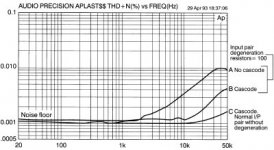
I haven't ignored the current mirror argument, I just haven't sat down and came up with a solution. I am perplexed at the size of some of the emitter resistors i see though, why so big? In Doug Self's article, he admittedly "over degenerates" the input current mirror to show the VAS distortions, except that he "over degenerates" them with 100ohm resistors, AHH! Does this not mean havoc for your VAS running resistors on an order of magnitude higher? Maybe the EF stage is just very tolerant...
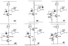
I post figures from his online article below only because I haven't yet grasped the issue. A picture of a test setup, a picture of the multiple Vas options - of which he proceeds to test the Cascode version, and Finally a picture of the emitter degeneration effects on a Cascode.
The goal of the Overall VBias is obviously to stay constant barring thermal compensation, so one would think that the Vbias after the drivers would have a similar fate? Well from inspection, it looks like the 100ohm driver base could cause an issue with varying current and thus voltage at the base, based on the transistors nonlinear output/input. However in practice I've also measured that this voltage across the outputs is not constant, especially not using a typical .22uf speedup cap there (at least not for me).
If I think hard enough I might find another reason to do it the CCS way. Possibly because it fixes the driver steady state current which is no longer dependent on any voltages staying constant at the output bases (or not). Now if we think about that, what happens?
If the output transistors are pulled low by a current source then all we must say for the output bias current is that the driver output current is equal to Current source current + Desired Output Bias Current/Beta. This seems a simple enough task, right?
Thus the voltage across the output pair has disappeared from the equation for output bias currents!!!!😱 Am I being stupid? It will be set according to the aforementioned currents at whatever voltage level works out, because we no longer enforce a 1.2V drop between the NPN and the PNP output transistor, they are separated as needed by the CCS's. Now let me see what I can gather from that.
I believe this means that we can now stabilize the output stage using only the drivers and the bias on a separate heat sink. And possibly if the bias currents are chosen well and the drivers are appropriately oversized, we might get rid of the need for thermal compensation!
This might also be an argument for running more or less current though the drivers:
1) One could think, less current!, because you could have hopes of keeping the drivers cool all the time, which might prove fruitful for low power amps or high beta outputs
2) Or one could exclaim, more current!, in the hopes of keeping an external heatsink closer to the same temperature under no load and load and thus relying less on thermal compensation.
Am I being crazy here or does this actually work?
Current Mirrors
I haven't ignored the current mirror argument, I just haven't sat down and came up with a solution. I am perplexed at the size of some of the emitter resistors i see though, why so big? In Doug Self's article, he admittedly "over degenerates" the input current mirror to show the VAS distortions, except that he "over degenerates" them with 100ohm resistors, AHH! Does this not mean havoc for your VAS running resistors on an order of magnitude higher? Maybe the EF stage is just very tolerant...
I post figures from his online article below only because I haven't yet grasped the issue. A picture of a test setup, a picture of the multiple Vas options - of which he proceeds to test the Cascode version, and Finally a picture of the emitter degeneration effects on a Cascode.
Attachments
Last edited:
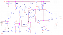
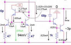
I figured out that I had missed something on the current mirror check I did last night, I must have just been tired because it seems obvious now.
Picture posed below.
Assume 2ma through both sides of the current mirror. (perfect symmetry)
Assume 6ma through the VAS (output zero condition - Steady State)
Vas needs 30uA to pull the 6ma (Gain = 200). Also it will create .625V on its base.
Thus the Vas Driver needs to output 30uA + .625V/1kohm = 30uA+625uA = 655uA.
The Vas driver needs 3.275uA to pull the 655uA (Gain 200). Thus the current mirror must also pull 3.275uA which will cause it to output 655uA. 20uA of this will be used for the base currents (2*10uA) and the rest must be shunted, so 635uA needs to go away.
Using the 47ohm Resistors I get 94mV across the resistors + .625V for the transistor and I come up with 1132ohms. Yay, a respectable number!
So now to make a simple equation for perfect symmetry under no signal conditions using a current mirror with a buffer, and an EF VAS stage.
Current Source Pulldown Resistor =
(I_Tail / 2 * R_CMirr + .625)/[(.625/R_PullD + I_Vas/Bv)/Bv*Bc-I_Tail/Bc]
Where:
I_Tail is the tail current
R_Cmirr is the current mirror emitter resistor
r_PullD is the VAS driver pulldown resistor
I_Vas is the CCS value from the VAS stage
Bv is beta of the VAS transistors
Bc is beta of the Current mirror
This can be highly simplified for normal values of the pulldown resistor. Assuming it is significantly small and the Betas are significantly high.
0.8*R_PullD*Bv/Bc*(I_Tail*R_CMirr+1.25)
which evaluates to 1150ohms which is as close to 1130 as you will get for normal resistance values. Looking at this, as R_CMirr goes up, so does the correct current mirror pulldown.
This is all of course assuming that the correct thing to do is to match the currents at zero signal... Which I think is still being argued. However, the voltage matching at the top of the transistors is obscured by the ability to read a difference, more likely to come from the emitter resistors being slightly different.
When Cdom comes into play at higher frequencies the whole analysis goes out the window because you will be pulling the current to control the drivers through the low impedance Cdom. I think this is where high frequency distortion comes from, the only way to stop it is to have a powerful input stage or have it buffered from Cdom somehow. This distortion is where I believe that the emitter Current mirror resistors will need to be small in order to be able to shunt this driver current. Possibly, this makes an argument against the EF stage and to the Buffered VAS stage.
Next Idea? We'll see later.
Attachments
Last edited:
I would need to check again, but first read through, indicates you understand where the currents are going and why they are certain values.
Once you can estimate the currents, you can move on to voltages and resistances.
Now you are ready to use a simulator to do all the arithmetic and you use your brain to ask the right questions.
Look up cascoded VAS and see why the cascode can offer advantages that suit the current demands from the LTP stage.
BUT,
the cascode has a high output impedance. This demands an EF or a three stage output using pre-drivers, or maybe both!
Going back a post to Self's 6 VAS options.
I think D+E is superior to C and all the others. F may be a close second.
Look around this Forum for good VAS stages that involve extra transistors as implemented by our experts.
Last edited:
Thanks AndrewT.mirror 3 is set up wrongly, if you ignore the extra resistor and transistor in the mirror.
The I1=0.4mA must equal the IbVAS + Ir2, since the same transistor is used for the EF and for the mirror.
Ir2~0.6V/330ohms
So if I correct Mirror3 maybe performance can match the Mirr1 and Mirr2.
Now I find your suggestion a bit unclear. It is probably my english.
Tell me what resistors to change and new values.
I will then ask my sim what it thinks abou it.
To optimise I tried several different alterations.
The diagram shows the lowest THD I could get.
----
When speaking of mirrors I think we must distingues between things:
1. DC-precision
2. AC-precision and distortion.
The best performance THD need not have the absolut uA precision.
There are other circuits than audio amplifiers
where we measure things. Here we should go for max current precision.
Last edited:
I was looking at the type E VAS and I think will try that next mainly because of the comment I had made before about separating the input pair from the drivers. When Cdom comes into play the input pair might have to directly control the drivers in an EF setup, but with a buffer I think it should be more linear and have more gain in the high frequency ranges.
I am going to build the amp with a type E VAS as it stands and maybe then if I am happy I will prototype a final board.
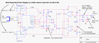
Protection Circuit
I am already on to more drawings. I have created a layout of a "Anti Thump" and a DC Offset Detector using a 555 timer and a dual op amp package. Might anyone have some suggestions to my madness? I have stolen ideas from circuits I have seen, but I'm ok with that.😛
The Idea is to turn on the relay with the 555 timer by making the output go LOW. Under startup conditions, the trigger will be low because it will still be charging its capacitor thus the circuit will start off correctly and the output will be HIGH. The output will stay stable until the 7Sec Threshold Cap charges, then it will go LOW and remain there until the circuit is restarted by pulling the trigger low again.
I use the op amps to intentionally pull the trigger low by use of an NPN transistor connected to their output. If either of the Op amps turn on (go High) then the NPN will discharge the caps and the circuit will turn off the Relay. If the Fault was hit by accident, then the circuit will just wait 7 seconds and re-engage. However as long as the op amps show DC voltage above 1.5V the circuit will stay off. The input Cap and Resistor were chosen for a low frequency filter and to separate the capacitor from the output. 80k might not be enough but I started there...
What do you think?
I am going to build the amp with a type E VAS as it stands and maybe then if I am happy I will prototype a final board.
Protection Circuit
I am already on to more drawings. I have created a layout of a "Anti Thump" and a DC Offset Detector using a 555 timer and a dual op amp package. Might anyone have some suggestions to my madness? I have stolen ideas from circuits I have seen, but I'm ok with that.😛
The Idea is to turn on the relay with the 555 timer by making the output go LOW. Under startup conditions, the trigger will be low because it will still be charging its capacitor thus the circuit will start off correctly and the output will be HIGH. The output will stay stable until the 7Sec Threshold Cap charges, then it will go LOW and remain there until the circuit is restarted by pulling the trigger low again.
I use the op amps to intentionally pull the trigger low by use of an NPN transistor connected to their output. If either of the Op amps turn on (go High) then the NPN will discharge the caps and the circuit will turn off the Relay. If the Fault was hit by accident, then the circuit will just wait 7 seconds and re-engage. However as long as the op amps show DC voltage above 1.5V the circuit will stay off. The input Cap and Resistor were chosen for a low frequency filter and to separate the capacitor from the output. 80k might not be enough but I started there...
What do you think?
Attachments
Last edited:
hi,
I can't read the diagram clearly.
Are the two opamps set up as a window comparator?
If so, then this is an excellent way to detect and trigger for excessive output offset.
Zener protection across the opamp inputs would allow more sensitivity of the DC detection with a much lower input attenuator. You may be able to omit the 10k completely. The 0.8s filter will then be loaded with a much higher impedance load than the present 50k. This seriously compromises the existing 82k filter's response.
This then lets you change the component values of the filter from 82k/10uF to ~470k/1uF with virtually no leakage current through the non existent electrolytic.
Last edited:
- Status
- Not open for further replies.
- Home
- Amplifiers
- Solid State
- Combined Topology - Thoughts?