Hi All,
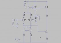
This is really getting on my nerves.... It is not immediately obvious to me as to what turns the Vas on into active mode in the below circuit. Obviously approximatly 0.7Vbe is what is required but how is that voltage generated? Should the collector of T1 (LTP output) be set somehow to provide the voltage? If so how does one set the DC voltage there? Can the current source of the Vas force it on? What are the mechanisms here?
I have had problems with my designs in simulation (LTSpice) whereby the Vas is either hard on and driving the outputs likewise, or it will not turn on without signal and not conduct quescient current. I have D. Self's book but it really doesn't say how the Vas is usually biased on (I presume its just a like a class A amp). Maybe I am missing something basic or just looking at this the wrong way but can anyone help?
Attachments
I would change in Q1, Q7 and Q8.
First, replace Q7 with two 1N4148 diodes in series. To make one 1.2V reference.
Bias them via one resistor to like 2 mA.
You can use R8 for this. Make it 15k. (35V/15k ~2mA)
From two diodes you attach to Q1 and Q8 bases, B-pin.
Now you have like 1.200V - 0.650V = 0.550V at those transistor E emitters.
And finally you can set the current. Via resistors from Emitters to +Volt supply.
Example.
Putting one 120 Ohm resistor to Q1 emitter
will give a constant current source (CCS) with
0.550V/120 Ohm = 4.58 mA
Each transistor in input pair will now run 2.29 mA
The trick is called feedback.
in the final circuit it will be applied and it will regulate the vbe such that the output voltage is where the input tells it to be.
without it you have a "hard time" tuning the inputvoltage to the value needed to have the VAS put out an intermedeate voltage that is neither the maximum or minimum voltage (close to the supplies).
but thats exactly how it is supposed to be, because it is the result of the high voltage gain, that you wish to have, so you can apply a lot of negative feedback to correct nonlinearity induced errors.
Hi thanks a lot krachkiste! This makes sense to me and was what what I originally thought (kind of) until I could not explain why the amp circuit below did not work. Basically the output stays at the negative rail voltage and is being driven there by the Vas. There is voltage at the diff amp Q12 base indicating the feedback signal is present from the output (almost negative rail). Therefore I do not understand why the output of the diff amp is not trying to drive the Vas to compensate this (like a feedback loop should!?!). Any ideas?
Attachments
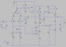
Hi Thanks lineup also. I have to say I don't really see what is wrong with the double current mirrors (Q1 and Q8 being mirrors of Q7) as being the current source for the diff Amp. Maybe I could see the Vas Current Source arm temporarily being turned off from a very large voltage swing so perhaps its a bad choice for that reason. Do you (or anyone else for that matter) think there any reason why the biasing diodes option is better the the current mirror set up I've got there (apart from the fact that in most cases the LTP current and the Vas current will not be required to be equal).
Hi thanks a lot krachkiste! This makes sense to me and was what what I originally thought (kind of) until I could not explain why the amp circuit below did not work. Basically the output stays at the negative rail voltage and is being driven there by the Vas. There is voltage at the diff amp Q12 base indicating the feedback signal is present from the output (almost negative rail). Therefore I do not understand why the output of the diff amp is not trying to drive the Vas to compensate this (like a feedback loop should!?!). Any ideas?
first choose some good models , I notice you have no model for Q14 , 11 , etc.
Since it looks like a basic self amp , here is one for you.. (below) unzip to folder , click and run. Observe (probe every point , you will see the scheme.)
OS
Attachments
Cheers ostripper, nice amp.
Just to make sure LTSpice was doing its job correctly, I made the exact same amp (except the models which I kept all as ideal) as my original in LTSpice and the thing worked fine! Perhaps with all the chopping and changing I have done with this amp over the last few weeks something has corrupted like one of the models or something? On the original one the -39V just does not leave the output no matter what I do.....maybe I will just ground it to teach it a lesson!
Just to make sure LTSpice was doing its job correctly, I made the exact same amp (except the models which I kept all as ideal) as my original in LTSpice and the thing worked fine! Perhaps with all the chopping and changing I have done with this amp over the last few weeks something has corrupted like one of the models or something? On the original one the -39V just does not leave the output no matter what I do.....maybe I will just ground it to teach it a lesson!
Do you (or anyone else for that matter) think there any reason why the biasing diodes option is better the the current mirror set up I've got there (apart from the fact that in most cases the LTP current and the Vas current will not be required to be equal).
Using just mirror without resistors to set the current
will be very difficult to predict how much current.
Such a mirror may work, or not, in SPICE.
But in real life there are practically not 2 transistors that are the same.
So your current would be terribly un-precise.
Using some VREF, like Diodes, RED LED + one resistor is what everybody use
to be able to set CCS current source with precision.
Using some VREF, like Diodes, RED LED + one resistor is what everybody use
to be able to set CCS current source with precision.
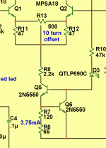
OR , 2 transistors with a trimmer (R6) to adjust CCS for best LTP operating point (most linear Ic). 😎
OS
Attachments
Are you sure Q9 is supposed to be a pnp?
I havent seen a vas configuration like this before, and i haven't put much effort in understanding it.
But I'm certain with the VAS configuration of post#1 it would work like it should.
PS:
Ah, ok, it seems to be a buffer to drive Q8. Should actually be ok.
sorry for the fuss
PPS:
what happens when you connect the collector of Q9 to negative rail?
if the output sticks to negative rail, then Q8 might be drawing too much current, and the question is why.
maybe it cant reduce its current below the ccs-current for some reason.
Last edited:
OR , 2 transistors with a trimmer (R6) to adjust CCS for best LTP operating point (most linear Ic). 😎
OS
Yes, you are right of course, ostripper.
Using 2 transistors is great!
Thanks for the constant current source revision lesson.....I needed it!
Now to incorporate these into my designs and also to stop questioning the magic of the feedback loop and I will be well on the way to understanding the black art of amp design....well at least the fundamentals....
Oh and to krachkiste, I tried tying Q9 to the negative rail and it didn't seem to do too much at all. On my working amp design it still worked. On the the broken one it was still broken. Didn't look any further into it than that.
Thanks everyone for their help. Truly is a great site!
- Status
- Not open for further replies.
- Home
- Amplifiers
- Solid State
- Vas DC Bias conditions?