Hi,
I was wondering why, in pre-complementary days, the all-PNP push-pull stages always incorporated a capacitive coupling between the phase splitter transistor and the lower output transistor.
I see no definite advantage to this arrangement, on the contrary:
-It requires an additional electrolytic
-It is inefficient, as the base resistor of the output devices consumes drive, but does not contribute to the bias current of the driver.
-It could cause nasty dynamic effects, because under large signal condions, the capacitor will charge through the BE diode of the output transistor.
The pic shows a typical such stage; C2 is the capacitor in question.
So, why not get rid of C2, R1 and R6, and adjust the value of R4 to the new conditions?
Attachments
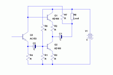
If you look at the diagram you will see that is powered by a single rail, on the union of the output transistors there is a voltage of Vcc / 2.
It is necessary to isolate the tension of the speaker, but otherwise he would be sending this DC and burn.
The effect of placing a capacitor in series with the speaker is compensated by the feedback network
It is necessary to isolate the tension of the speaker, but otherwise he would be sending this DC and burn.
The effect of placing a capacitor in series with the speaker is compensated by the feedback network
If you look at the diagram you will see that is powered by a single rail, on the union of the output transistors there is a voltage of Vcc / 2.
It is necessary to isolate the tension of the speaker, but otherwise he would be sending this DC and burn.
The effect of placing a capacitor in series with the speaker is compensated by the feedback network
I am talking of C2, not C1.
maybe to let the lower output transistor work as ccs, thus having a more stable idle current? or equivalent to make it able to work with a "window" of DC on the input,
with which it still functions. (this suggests the input is DC coupled to the previous stage, for some reason, perhaps global thermal stability or DC or so)
with which it still functions. (this suggests the input is DC coupled to the previous stage, for some reason, perhaps global thermal stability or DC or so)
So, why not get rid of C2, R1 and R6, and adjust the value of R4 to the new conditions?
Germanium transistors with lots of thermal issues?
It is a class B, not class A.maybe to let the lower output transistor work as ccs, thus having a more stable idle current? or equivalent to make it able to work with a "window" of DC on the input,
with which it still functions. (this suggests the input is DC coupled to the previous stage, for some reason, perhaps global thermal stability or DC or so)
And anyway, it doesnt change a lot of things: in one case the bias is provided
by R6, in the other it would come from R7 via Q3.
Yes, I didnt represent it, but R1 is made up of a NTC + resistor.Germanium transistors with lots of thermal issues?
But this composite could be adjusted in value and in "mix" to give an identical Iq and stability.
We're smarter now and it's just a matter of style and complexity. Back then designers tended to treat each active device as a block, getting the DC bias where they wanted it, and isolating the whole thing with caps. Today we have a lot more experience with direct coupled circuits and know the benefits (and pitfalls). I always think of my SWTPC Tiger amp, the first direct coupled circuit I worked on. When something failed, typically everything failed, as it was all tied together. One quickly learned to check every single device and to limit current on start up until all was well. You almost never have that problem with circuits using a lot of coupling caps to isolate the stages- failures are invariably local.
Yeah, it could be the reason. It's something I hadnt considered, as our forefathers are supposed to be so much smarter, but it is a possibility.We're smarter now and it's just a matter of style and complexity. Back then designers tended to treat each active device as a block, getting the DC bias where they wanted it, and isolating the whole thing with caps. Today we have a lot more experience with direct coupled circuits and know the benefits (and pitfalls). I always think of my SWTPC Tiger amp, the first direct coupled circuit I worked on. When something failed, typically everything failed, as it was all tied together. One quickly learned to check every single device and to limit current on start up until all was well. You almost never have that problem with circuits using a lot of coupling caps to isolate the stages- failures are invariably local.
What is going to happen?well, it definately stabilizes the idle current more (heat q3, what happens?)
Q3 will conduct more, feed more current into Q2 and divert the same amount of current away from Q1.
This will cause a shift in the average output voltage, but in principle, the overall DC feedback will try to compensate this shift.
This may look counter-intuitive, but the Iq will not be affected.
The only parameters that can affect the Iq are the Vbe of the output transistors, and the current through R7 (refered to the mid-supply voltage).
It is the circlotron or virtual complement principle.
First - my take on it. I think it is a question of level shifting and bias. Germanium transistors have turn on voltages of .2 to .3 volts, which is where the base of Q2 would sit. Would mean that not much signal would cause distortion in the drive transistor. Also, they may want to keep the idling current low in the drive transistor, leaving the capacitor to function similar to an emitter by-pass. I think also, the designs at that time were trying to keep number of semi-conductors to a minimum, which means use coupling caps or transformers instead of more transistors. My 2 cents.
well, i have no spice now, but to me q2 sets the idle current, and q1 complies to it. in the schem, it is not influenced by the DC point of q3. if DC coupled, q2 and q3 multiply beta like a darlington, and become very sensitive to DC point (and thermal bias).
where is the ground reference actually? (i assumed the bottom rail)
edit: i do not like this schem at all ;p, but i honestly do think there is a technical function for that cap coupling.
plus, i guess it has something to do like this, heat q3, it draws down the B and E of q1,
thus the voltage over q2 and it's dissipation diminishes as well.
Last edited:
such, that Pd of q1 remains equal, but Pd of q2 decreases, thus total Pd decreases, the stuff cools down (and q1 Pd drops after all) ;p
The absolute value of the Vbe (or bandgap, to be more accurate) is mostly irrelevant, as long as all devices homogeneous, and the components values take it into account.Germanium transistors have turn on voltages of .2 to .3 volts, which is where the base of Q2 would sit. Would mean that not much signal would cause distortion in the drive transistor.
You are right, in some respects: this example runs on one leg, because Q1 has no B-E resistor.well, i have no spice now, but to me q2 sets the idle current, and q1 complies to it. in the schem, it is not influenced by the DC point of q3. if DC coupled, q2 and q3 multiply beta like a darlington, and become very sensitive to DC point (and thermal bias).
where is the ground reference actually? (i assumed the bottom rail)
edit: i do not like this schem at all ;p, but i honestly do think there is a technical function for that cap coupling.
plus, i guess it has something to do like this, heat q3, it draws down the B and E of q1,
thus the voltage over q2 and it's dissipation diminishes as well.
Some implementations of this topology do have that B-E resistor, though not necessarily identical to that of Q1.
Which is problematic, because equality is required for true circlotron operation.
Maybe this point was missed by early designers, which is why they felt the need to use a capacitive coupling.
The question would be worth asking a designer of that time: I'm particularly thinking of Herman Schreiber: he certainly is a clever guy, and wouldn't throw any component value or circuit configuration without a good, rational reason.
Is someone in contact with him?
Back in the early days of transistors designers knew how to design good, working tube circuits that always had a large voltage difference between amplifier stages. These stages were always linked with coupling capacitors. In the beginning because designers had little experience with transistors they just adapted their tube designs for transistors. This often resulted with the first solid state components that replaced their tube counter parts to actually perform more poorly than their Tube predecessors. One good example of this was the Marantz 7C, a good tube pre-amp and the Marantz 7T it’s solid state replacement.
- Status
- Not open for further replies.
- Home
- Amplifiers
- Solid State
- Reason for capacitive coupling in vintage push-pull stage