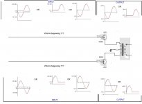
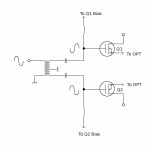
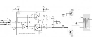
I am confused as to how exactly the waveforms function when using a phase splitter transformer like in the zeus amp , this tramsformer is driven class a open ended type , what do the voltage waveforms look like , reference to center tap . My drawing is simply similar to the zeus amp with input transformer missing and waveform shown .
Plz enlighten me from the image I made , wich of these is the corrent interpretarion .
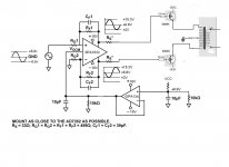
Also , can this be done with an op amp or any source that is driven from a seperate yet lower voltage power supply .
thx you
Plz enlighten me from the image I made , wich of these is the corrent interpretarion .
Also , can this be done with an op amp or any source that is driven from a seperate yet lower voltage power supply .
thx you
Attachments
Last edited:
...what do the voltage waveforms look like , reference to center tap...
Ask and ye shall receive (see attached)
Since this is a Class A amp, each final has a duty cycle of 360deg. The phase of the output depends on the phase of the OPT, and how the finals are connected. If this used gNFB off the secondary (which it doesn't) and you had positive feedback, you could change that by reversing the connections at the primary.
The phase splitting IST simply gives two signals 180deg out of phase, and (hopefully) of equal magnitudes.
Also , can this be done with an op amp or any source that is driven from a seperate yet lower voltage power supply .
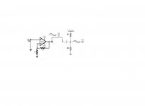
See Here, Fig 24. This is how to implement a paraphase splitter with op-amps.
Attachments
Miles thx you for your response .
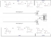
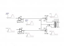
One simple question , those 2 out of phase pics with the mosfets .
What are they referenced too . Imagine this as it were dc .
Are they floating at around + 2 volts ? Or are each waves from the transformer to center tap real AC , real alternating electrons like like wall current . This seems to be so from the ac books i read .
here is the zeus amp
http://www.tubecad.com/2004/image097.gif
Last edited:
What are they referenced too . Imagine this as it were dc .
Are they floating at around + 2 volts ?
The input AC rides on whatever the DC gate bias happens to be to set the no-signal bias current through the finals. That might be around 2.0Vdc, depending on what MOSFETs it uses.
When you say the ac signal rides on top of the dc , would that look more like the lieft most or the right most of the input pics .
thx you
What if both devices are not entirely matched , how can I bias them individualy ?
thx you
What if both devices are not entirely matched , how can I bias them individualy ?
When you say the ac signal rides on top of the dc , would that look more like the lieft most or the right most of the input pics .
The left most one.
What if both devices are not entirely matched , how can I bias them individualy ?
You'd have to capacitor couple the inputs so each MOSFET would connect to its own bias network. For current matching, you would include a small current sense resistor in each source lead, usually 1R will do nicely for that. You could also use the Rdc of the OPT as a current sense resistor, but beware that the resistance of each side of the center tap won't be equal.
Attachments
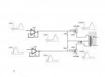
Ok my next question is , Altho I believe I know the answer , the voltage waveform from sourre of mosfet buz901 referenced to center tap will look like the right most ? correct ?
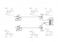
My next question is this , what if i were to get nearly matched mosfets and use this technique , see pic , is this good , i I read everywhere that differential is the way to go for phase splitting but I dont understand well ,
http://www.diyaudio.com/forums/chip-amps/126529-balanced-unbalanced-preamplifier.html
my anwer to these people , show me the schematics !!!!
I modified a circuit , see pic attached , is this good ? Could this work ? modified from this .
http://www.analog.com/static/imported-files/images/verified_circuits/CN0040_00_1024.gif
I read somewhere that lateral mosfets really thrive with high voltage 30 ish voltage , problem is theres no good components reaching those , I wanted to use 28 volts I guess 13 volts will do . Either get better signal driving with less mosfet thriving or more happy mosfets and worse signal ... ??
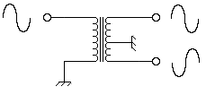
Also , plz answer this question for me , I am dying to know , what is , is there , a difference between these 2 configurations when using an center tap output transformer push pull type .
http://sub.allaboutcircuits.com/images/03474.png
http://www.tubecad.com/2004/image097.gif
Thx you
My next question is this , what if i were to get nearly matched mosfets and use this technique , see pic , is this good , i I read everywhere that differential is the way to go for phase splitting but I dont understand well ,
http://www.diyaudio.com/forums/chip-amps/126529-balanced-unbalanced-preamplifier.html
my anwer to these people , show me the schematics !!!!
I modified a circuit , see pic attached , is this good ? Could this work ? modified from this .
http://www.analog.com/static/imported-files/images/verified_circuits/CN0040_00_1024.gif
I read somewhere that lateral mosfets really thrive with high voltage 30 ish voltage , problem is theres no good components reaching those , I wanted to use 28 volts I guess 13 volts will do . Either get better signal driving with less mosfet thriving or more happy mosfets and worse signal ... ??
Also , plz answer this question for me , I am dying to know , what is , is there , a difference between these 2 configurations when using an center tap output transformer push pull type .
http://sub.allaboutcircuits.com/images/03474.png
http://www.tubecad.com/2004/image097.gif
Thx you
Attachments
Last edited:
Ok my next question is , Altho I believe I know the answer , the voltage waveform from sourre of mosfet buz901 referenced to center tap will look like the right most ? correct ?
Not if it's Class A, then it will look like the ones on the left. What you've got for the right-hand outputs is Class B, and that's really hideous for audio, and should be used only where you need lotsawatts and efficiency, not sonic excellence.
My next question is this , what if i were to get nearly matched mosfets and use this technique , see pic , is this good , i I read everywhere that differential is the way to go for phase splitting but I dont understand well , my anwer to these people , show me the schematics !!!!
For phase splitting, your only real choices are either a differential splitter or a cathodyne. Paraphase splitters in all their various iterations are more in the "quick 'n' dirty" category. So far, I've implemented these with vacuum tubes, and not solid state yet. The hollow state differential features excellent phase-to-phase balance, and sounds just great.
is this good ? Could this work ? modified from this .
Depends. I don't have any experience with that particular IC. May be someone here knows better about that dealie.
I read somewhere that lateral mosfets really thrive with high voltage 30 ish voltage , problem is theres no good components reaching those , I wanted to use 28 volts I guess 13 volts will do . Either get better signal driving with less mosfet thriving or more happy mosfets and worse signal ... ??
It's better to give the MOSFET finals a higher voltage to keep 'em away from the rails. Internal MOSFET capacitances do some squirrelly things when Vds drops to a very low value. See MOSFET spec sheets for this.
Also , plz answer this question for me , I am dying to know , what is , is there , a difference between these 2 configurations when using an center tap output transformer push pull type .
http://sub.allaboutcircuits.com/images/03474.png
http://www.tubecad.com/2004/image097.gif
Both of those are equally horrible, Class B types that will sound like
An externally hosted image should be here but it was not working when we last tested it.
due to the cross-over distortion these will produce. Best to reserve these types of finals to RF, where you can rely on LC tuners and/or bandpass filters to remove the harmonic distortion. You definitely don't want that in an audio final.Hi , thx for all the response ,
when I showed these pic , I was just asking myself why one has grounded center tap and one has b+ center tap , sorry for not being clear enough .
http://sub.allaboutcircuits.com/images/03474.png
http://www.tubecad.com/2004/image097.gif
So the zeus amp with the input transformer has class b output ? , is what I was trying to say , the output waveform will be that of the right most ? , since mosfets dont work when there is reverse voltage ? It has continuous bias of 500mV distortion wont be so bad right ?
Yes mmmmmm....tasty.... phase splitters , any schematics ?
I will be going class a myself , I want the purest of ac sinewaves , with pure sinus current as well .
I thought mosfets liked going close to the fail and clipped smoothly ?
Not going to the rail = more power wasted , I am gonna ( try ) to use all i got .
Last edited:
Hi
One thing to keep in mind is that Av of the inverting op-amp is -(Rfb/Rin) and for the non-inverting op-amp Av is 1+(Rfb/Rin). For a proper phase splitter -Av should equal +Av.

One thing to keep in mind is that Av of the inverting op-amp is -(Rfb/Rin) and for the non-inverting op-amp Av is 1+(Rfb/Rin). For a proper phase splitter -Av should equal +Av.
Hi , thx for all the response ,
when I showed these pic , I was just asking myself why one has grounded center tap and one has b+ center tap , sorry for not being clear enough .
http://sub.allaboutcircuits.com/images/03474.png
http://www.tubecad.com/2004/image097.gif
One is a source follower operating off a positive rail, and so needs to have the sources at DC ground. The other one is a grounded emitter design that needs a positive rail for the collectors.
So the zeus amp with the input transformer has class b output ? , is what I was trying to say , the output waveform will be that of the right most ? , since mosfets dont work when there is reverse voltage ? It has continuous bias of 500mV distortion wont be so bad right ?
Last I heard, the Zeus is Class A, and so each phase operates with a 360deg duty cycle and reproduces the entire waveform. For source followers, that "reverse voltage" doesn't matter since the gate and source are at nearly the same potential at all times.
I thought mosfets liked going close to the fail and clipped smoothly ?
Not going to the rail = more power wasted , I am gonna ( try ) to use all i got .
Well, they don't. Take a Look, see at the characteristics. Pay particular attention to what happens to internal capacitances as Vds drops to small values. It ain't pretty. Better to trade some power for improved sonic performance.
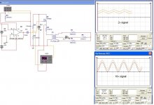
Ok I think I get it now , so this is a drawing . Sorry for my original picture untitled33 the left most input was wrong .
So do I get it now ? Look at image untitled36 . Once I
Ok it seems like you misunderstood my question , I know that this is a follower , what I am asking is , Is there a difference with the magnetic fields when the center tap of the primary is b+ or ground , does it do the exact same thing , only one is used because mosfet is a current source in this particular circuit and somestimes we use npn sink both in opposing directions , but does it change anything one config or the other ? That was the nature of my question . Sorry for now being clear.
Lateral mosfets do have soft clipping , this may or may not be an overrestimated but I wont be leaving too much headroom thats 4 sure . I hear from class d these new mosfets are extremely linear and very rugged .
http://www.semelab.com/magnatec/alfet.shtml
Attachments

Last edited:
Ok I think I get it now , so this is a drawing . Sorry for my original picture untitled33 the left most input was wrong .
So do I get it now ? Look at image untitled36 .
Yes, you got it now.
Ok it seems like you misunderstood my question , I know that this is a follower , what I am asking is , Is there a difference with the magnetic fields when the center tap of the primary is b+ or ground , does it do the exact same thing , only one is used because mosfet is a current source in this particular circuit and somestimes we use npn sink both in opposing directions , but does it change anything one config or the other ? That was the nature of my question . Sorry for now being clear.
It makes no difference. In both cases, the primary center tap is at AC ground since the opposing currents cancel at the center tap.
Lateral mosfets do have soft clipping , this may or may not be an overrestimated but I wont be leaving too much headroom thats 4 sure . I hear from class d these new mosfets are extremely linear and very rugged .
Magnatec. ALFET Lateral MOSFETs
Another case of try and see. When I do solid state designs, I prefer overdesigned power supplies. I have one that could legitimately be marketed as a 12W design, but I restrict it to no more than 3.0W out. Sounds better than almost any "Big Box" SS amp.
So , hypotheticaly , in a bare bones perspective .
Could op amps do the exact same thing if configured as this if proper signal was provided to the buffer amps ? Or to the currents just cancel eachother at the central node like in a diff amp asymetry test ... I am confused ....
It seems to me like I could adjust the bias before the buffer instead of using ac coupling on the line driving the power mosfets right ? .... bad right ...
using seperate power supplies , +-18 regulated and 2 x series batteries . same ground for all .
Here is another of my images , can this work , is this functionnal and the exact same thing ( quality aside ) as the transformer phase splitter ...
Today I had a design idea type of thing , I was finally understanding things... while I was putting cans on the shelves at my job ... one step @ a time .... slowly .... slow ...
Attachments
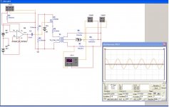
Here are some few observations I made , picture 39 , 40 and 41 . Perhaps sticky this as a "noob visualisation of a phase splitter for dummies" . For thoese who still wonder how these actually work plz look .
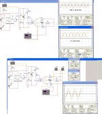
So what is mindboggling to me is pic untitled40 , there is an ac like voltage between probe a and ground yet after that resistance , probe b , there is nothing but dc , strange indeed , I guess this is how it works since they are cancelling out ...
So basicly I see now that the zeus pic with the 2v battery is just for example purpose , 2 volt will never be enough with a high swinging signal lets say +-15 , this cant be as the wave in my post above pic untitled36 centered around +2 volts and giving such an output at the mosfet ?? it has to be completly over ground , example the 12 volt battery simulation . I didnt test with the 2 follower after the phase splitter , but 2 volt wont work right , or am I missing something or not understanding something ?
Was Miles Power wrong or right in his post above when referring to the output pic untitled36 ? .
Also I notice something with class a , plz refer to pic untitled 39, lets say I wanted to amplitude modulate a signal with a class a type amp , am I gonna get for a short moment the floating dc divided by the primarys winding resistance ? I could have 5 volts dc sometimes , that could be very high amps ... Or would the amplitude modulation actually be affected by the reactance since it is not really a static floating dc but a modulated one ? Is the question clear enough ? ..
So I decided that I would bias the 2 mosfets from the same source and try to avoid capacitor coupling , the Vgs of lateral mosfets dont vary as badly as I tought .
Also I have the this poop circuit with a drv134 , picture drv134poop , based on this post , pic from post #3 by leadbelly. Plz say what you think about this .
http://www.diyaudio.com/forums/chip-amps/126529-balanced-unbalanced-preamplifier.html
Could this make a functionnal phase splitter ? Is this thing too unstable if both half circuits with are not exactly same impedance/resistance , these mmosfets capacitance could vary and the transfo impedance as well ... ? I just want the voltage at the mosfet gate to the same basicly ... Personally I dont understand this circuit , It seems like it would be simpler to just use a regular op amp inverting and non inverting but I read this is no good ...
So I hope somebody can read this blabbering and comment to my observations/questions .
Attachments
Last edited:
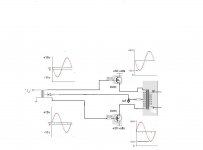
So assuming the mosfet has a Vgs of 1.5 volt , does pic untitled 36 make sense or no ?
Also I minda worried about this , looking at this now based on these sims , how do you keep the amp from breaking at low volumes with so high bias ?
Is this how people bias class a or am I missing something ?
I almost feel like trying this out ... I need an active rectifier of immense speed and symetry and then bias that , and then buffer it with an op amp .
How bout a design like this ? Has something like this ever been tried ?
Attachments
I can't see how an input of +28V to the opamp can give an output of +28V if the supply is limited to +18V.
Surely your opamp is specified for a maximum range of acceptable input voltages and also damaging input voltages.
Surely your opamp is specified for a maximum range of acceptable input voltages and also damaging input voltages.
Hi, you also need to use some transistor for driving the mosfet, that able to give at least +37V while driving your mosfet at full output. To reach 30V at its source, and Vgs 7V, the driver should able to have 37V output. Also place some zener to protect the mosfet gate.
O my mistrake , I didnt realise , What I meant to do was the following , does this make sense ? see pic below , will this do as picture shows if vgs was 1.5 volt
I almost feel like trying this out ... class b type a push pull transformer coupled ...I need an active rectifier of immense speed and symetry and then bias that , and then buffer it with an op amp .
Yes zeners ... thats good ... these mosfets dont have any internal ones .
I dont think lateral mosfets have a vgs of 7 volts , datasheets says 0.4 to 1.5 vgs .
Also I was wondering , , lets say I go for class a with massive bias , how can I start the amp this without damaging it ? It seems to me like the signal must be in full swing before I connect the power to the mosfets otherwise if there is no signal and power is there there will be pure DC ... ?
I guess I need to start signal then cpnnect leads ? .... sounds strange . Is this how it is usually done ?
Attachments
Last edited:
- Status
- Not open for further replies.
- Home
- Amplifiers
- Solid State
- Few question , plz help