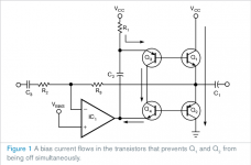
Here is the output stage WITH the 20 ohm resistor added. I also added the large cap across that resistor, as that was mentioned. I'm sure the value won't be what someone else would have used, but we have already established, a few posts back, that part values don't matter.
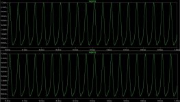
I have included a screen shot showing the output current minimum at 20 Hz at rated output power into 8 ohms. I show the value for an emitter resistor minimum. the blue trace is an NPN emitter. The green trace is for a PNP emitter. On the blue trace, the current is well above the spec sheet figure of 5uA max for cut off current. In fact, it is almost 100 times greater. The green trace has a minimum of about 1.13mA minimum.
I have also included the LTspice files so anyone can check this for themselves.
Attachments
Hardly surprising with a 8 ohm load, 4 pairs of output transistors and 0.1 ohm emitter resistors on +-34V. Vbe is still 460mV at its lowest excursion so of course there will be conduction. A standard triple EF does the same thing under the same conditions of load, power supply and emitter resistance.
The bias voltage (driver or output transistor base to base) varies a little over the cycle and actually it reaches its lowest point at this time. Still, thanks to the low emitter resistor voltage drop, the inactive side will still be conducting a little current because the BE junction is forward biased.
Reducing the load resistance to 2 ohms makes the current drop to 0 in your simulation.
automatic bias (EDN, December 2009)
Yet another mid-fi thingy: Class B amplifier has automatic bias - 10/22/2009 - EDN
Yet another mid-fi thingy: Class B amplifier has automatic bias - 10/22/2009 - EDN
Attachments
Running Steve's file in LTSpice, I notice one thing. At 20KHz for a normal EF there are jagged spikes before and after crossover in the Ib of the outputs. But here there's no such phenomenon even at 50kHz and nothing shows even at 500KHz... So apparently something good is happening here. Minimum current doesn't go under 1.8mA with the given load, so it looks like things are working.
I think it would be simple to throw together a real life prototype and o-scope it.
- keantoken
I think it would be simple to throw together a real life prototype and o-scope it.
- keantoken
Running Steve's file in LTSpice, I notice one thing. At 20KHz for a normal EF there are jagged spikes before and after crossover in the Ib of the outputs. But here there's no such phenomenon even at 50kHz and nothing shows even at 500KHz... So apparently something good is happening here. Minimum current doesn't go under 1.8mA with the given load, so it looks like things are working.
I think it would be simple to throw together a real life prototype and o-scope it.
- keantoken
I don't see this, I turned the four input devices into two darlingtons to make an EF output that was as little a change from the original as I could. The plots for the Ib of one output are almost identical.
Only one leg of four runs at ~220mA so thats 880mA for ~60W a channel idle, of course the output never switches off.
Attachments
Spent a little more time and made an EF and a couple of bias diodes out of the four input transistors. So now we have a triple EF. vs. original. Using nothing but the files posted just above I get .025% thirds with the TEF and .035% with the original. I was pretty careful to bias all devices close to the same currents. As it's biased now its smokin' class A.
steve, your output stage is basically a triple emitter follower
scheme, no matter the currents sources and the two transistors used
to provide bias...
so far, i (re) made some sims, and the result in matter of
crossconduction is the same as a triple emitter follower,
safe that this latter has lower distorsion...
current for power devices was set to 100 mA/transistor,
that make a 400 mA quiescent current, quiete extreme class ab..
I'm also comparing it alongside a darlington EF with normal bias and the EF is performing better. They both perform nearly the same into 2 ohms.
Sim file attached. Rename to .asc. To make sure I replaced model with Andy_C's models (included in the file), same result.
Someone with a scope will have to build it, or we'll only be able to argue about simulation (is it possible that faulty Vcbsat model parameters could cause this?). Until then, I don't see how useful discussion can be. (I have two good scopes and can test, but I'm not sure if I want to build it in my current situation. I'd be happy to test a prototype if available)
- keantoken
Attachments
Spent a little more time and made an EF and a couple of bias diodes out of the four input transistors. So now we have a triple EF. vs. original. Using nothing but the files posted just above I get .025% thirds with the TEF and .035% with the original. I was pretty careful to bias all devices close to the same currents. As it's biased now its smokin' class A.
I'm a little curious, of course you are aware of that by now.😀 Since I posted my file as I ran it, wouldn't it have been easier to use the one I posted instead of drawing up a new (different) one? Is there something wrong with the file I posted that some of you are trying to correct? By "thirds" do you mean the third harmonic? My results are different (using LTspice), very different. I also know that that the circuit measures much better than that, even with two pair of outputs running at about 1/4 that dissipation.
Could you post your file in LTspice format so I, and others here can check it for ourselves? Of course I could insist that you post it in my preferred program format. That would be more like the treatment I received from Andy_C and GK.
steve, your output stage is basically a triple emitter follower
scheme, no matter the currents sources and the two transistors used
to provide bias...
so far, i (re) made some sims, and the result in matter of
crossconduction is the same as a triple emitter follower,
safe that this latter has lower distorsion...
current for power devices was set to 100 mA/transistor,
that make a 400 mA quiescent current, quiete extreme class ab..
It looks like one of us has done their math wrong, or you are using a different circuit. Please post your simulation files in Intusoft format so I can review your rseults.
>I get .025%
And I get 33ppb with my amp 😛
So what? If you want to start a thread about your amp, feel free to do so. Going OT here will just result in those posts being pulled. I'm sure you'd rather have your stuff looked at, so...
I'm a little curious, of course you are aware of that by now.😀 Since I posted my file as I ran it, wouldn't it have been easier to use the one I posted instead of drawing up a new (different) one? Is there something wrong with the file I posted that some of you are trying to correct? By "thirds" do you mean the third harmonic? My results are different (using LTspice), very different. I also know that that the circuit measures much better than that, even with two pair of outputs running at about 1/4 that dissipation.
Could you post your file in LTspice format so I, and others here can check it for ourselves? Of course I could insist that you post it in my preferred program format. That would be more like the treatment I received from Andy_C and GK.
Please Steve don't create confusion when it's not necessary. To make it perfectly clear I ran your file with NO changes and YOUR models also with NO changes. I then used the same devices and rewired them as an ordinary Triple EF just to compare.
BTW there is no node "c" in your schematic so for the distortion analysis I labeled the output "c" I assume that was the intent?
OK I just did it again, posted below.
Attachments
Last edited:
It looks like one of us has done their math wrong, or you are using a different circuit. Please post your simulation files in Intusoft format so I can review your rseults.
there s nothing wrong...here the sims...
i used your models ,wich if my memory is good
were provided by andy_c, as i ve got them already in my
library...
the slight and non meaningful difference with a triple emitter
follower is due to your serial connected bjts used a variable
vbe devices for IQ current setting...
crossconduction range for a double emitter follower is about
10V, and adding a third emitter follower will extend this width,
so no wonder that the crossconduction range is greater,
whatever the circuit...
one thing more is that this crossconduction width is also
improved because of the smaller influence of vbe variations
when using 0.1R emitter resistors, along with the fact that
four transistors are used with each a 0.1R , reducing the
vbe variation greatly, but this will work, one more time,
whatever the output stage, krill or simple triple emitter follower...
i used 103 and 105 mA per power device, respectively for the
emitter follower and your krill...
with a Total Iq of 412 mA , no wonder that the two
topologies don t switch off easily...
i added fft s to compare distorsion, and in this respect,
the devices you use to settle the idle current seems to add
some nonlinearities....
conclusion will be the same that the one that did emerge
from the same debate some times ago, and can be resumed as :
the krill circuit has no effects on the switching behaviours
other than the ones already known for whatever output stage..
Attachments
One last plot (again the files from post #341 with no changes). The DC transfer function. The offset .123V, the gain ~.9909, the residual "S" shaped error consistent with mostly third harmonic at ~.03% or so. I would doubt this level of smooth low order distortion is audible certainly not at full power.
Attachments

Please Steve don't create confusion when it's not necessary. To make it perfectly clear I ran your file with NO changes and YOUR models also with NO changes. I then used the same devices and rewired them as an ordinary Triple EF just to compare.
BTW there is no node "c" in your schematic so for the distortion analysis I labeled the output "c" I assume that was the intent?
OK I just did it again, posted below.
I'm sorry if I appear to be confusing things, but I just don't understand how the same file, with no changes, run on the same simulation software, but on two different machines, can give such different results. Three machines if you count Edmond's result. I show a bias current 20% lower than what you reported, and 100% higher than wahab reports. He is using different software, and changed the value of 3 resistors in the schematic, so for now, we will only discuss the differences we got. You get an offset of 0.123V, I get an offset of 0.018V. There IS a C node in my schematic, I have no idea where it went in the one you downloaded. Every number, from THD, to each harmonic, is different between your results and mine. I can see where this could lead to some disagreement, and possibly a little confusion. At this point, it hardly seems worth continuing this discussion.
You get an offset of 0.123V, I get an offset of 0.018V. There IS a C node in my schematic, I have no idea where it went in the one you downloaded. Every number, from THD, to each harmonic, is different between your results and mine. I can see where this could lead to some disagreement, and possibly a little confusion. At this point, it hardly seems worth continuing this discussion.
I would agree with that I will go back to non-participation in this matter. BTW you have a DC offset of .123 V programmed into your sine source and if anyone opens the .asc file in the .zip in post #341 as text (you don't have to download it) you will see five FLAG directives four are 0 (gnd) and one is A, no C.
I would agree with that I will go back to non-participation in this matter. BTW you have a DC offset of .123 V programmed into your sine source and if anyone opens the .asc file in the .zip in post #341 as text (you don't have to download it) you will see five FLAG directives four are 0 (gnd) and one is A, no C.
The DC programed into the sine source is 0.116V, not 0.123V. I believe I covered that when I wrote:
Here is the output stage only. I simply deleted the VGS. Some of the node numbers were changed by the program when I did this. I have always used a higher voltage regulated supply on everything but the drivers and outputs, so I have left the 40V supplies in. If you choose to use only the 34V supplies, you will need to add the connections so the front of the OPS gets voltage. This will change the measurements I posted earlier, but not much. The DC on the input is to adjust the output offset. This was done before in the VGS. The 277 ohm resistor in series with the input represents the output impedance of the VGS. I put it there to be complete, it is not needed.
Andy did his sim with only the 34V supplies. I kept that change in my sims so our voltages would match.
Node C is labeled at the junction of R19 and R20. If you look at the parameters printed just below the sine source you will see the line that says:
.four{freq}V(c)
That line is also in the net list.
...
WIRE 544 1008 544 960
FLAG 2416 384 0
FLAG 544 -272 0
FLAG 544 1008 0
FLAG 624 176 A
FLAG 464 416 0
SYMBOL npn 864 224 M90
...
...
SYMATTR Value SINE(.12375 29 {freq})
...
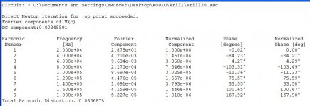
Circuit: * C:\Documents and Settings\swurcer\Desktop\AUDIO\krill\Krill20.asc
Direct Newton iteration for .op point succeeded.
.fourier quantity "V(c)" not pressent in data.
LT spelling not mine (this time).

WIRE 544 1008 544 960
FLAG 2416 384 0
FLAG 544 -272 0
FLAG 544 1008 0
FLAG 624 176 A
FLAG 464 416 0
SYMBOL npn 864 224 M90
...
...
SYMATTR Value SINE(.12375 29 {freq})
...
Circuit: * C:\Documents and Settings\swurcer\Desktop\AUDIO\krill\Krill20.asc
Direct Newton iteration for .op point succeeded.
.fourier quantity "V(c)" not pressent in data.
LT spelling not mine (this time).
- Status
- Not open for further replies.
- Home
- Amplifiers
- Solid State
- Krill - The Next Generation