Hello I have a perplexing problem and am hoping someone may be able to shed some light on the matter. First of all I am an electronic and computer engineer mainly specialising in digital design, occasionally dabling into analogue when I need a power supply for something. Analogue was never my strong point and BJTs always seemed a bit like black magic!
Any hows here goes...
I have a peavey pvx-125, schematic here: http://www.geminidj.com/disc._prod_manuals/AMPS/PVX-125/PVX-125.pdf
When the amp powers up it goes strait into protect. Now as I am aware this is either due to a problem with the DC bias or a problem with one of the output transistors supplying the rail voltage strait to the speakers.
So my first step was to test all the output transistors. They are 'SC3281' http://datasheet.octopart.com/2SC3281-Toshiba-datasheet-101323.pdf
Now as far as I am aware to check an npn transistor with a multimeter on diode mode you would check base(b) to (=>) Collector (C) then b => emitter (e). Both should read around 0.5 to 0.8 v.
I have checked the output BJTs they are (on the schematic) Q112, Q111, Q113 and Q212, Q211, Q213. I get the same result on each and every BJT. whn measuring B=>C I see 0.509v. When measuring B=>E I get 0.136v.
Are these values too far out? Is every single output transistor toasted here? They all have almost the EXACT same value.
I have also checked Q107 and Q207, I believe these are the DC stabilising transistors. They are 2sc3421:http://www.toshiba.com/taec/components2/Datasheet_Sync//66/7767.pdf
When measured in the same way (B=>C then B=>E) they show a good healthy 0.752v each. I see from the schematic that Q107 and Q207 are in a darlington pair configuration with Q106 and Q206 respectivly. There companion transistor read B=>C 0.8, B=>E 0.8v (the same for both).
In addition to this, I see that there is a potential difference of around 0.6v on each speaker output channel. (2 channels).
At my disposal I have a trusty old crt oscilloscope, a very nice function generator, multimeters and some power supplies.
So I am a little stumped. What could be going wrong? Bear in my mind I that this is the first time I have tried to repair an amplifier of this complexity. I have done plenty of work with small battery powered D class amps, but this is a whole other league! So please any suggestions no matter how obvious they may seem.
Thank you
Are these values too far out?
Are you measuring with the parts still installed? Sounds a lot like it. Because then you get identical readings for the outputs because they are paralleled.
You can't reliably measure the parts still installed, you have to take them out.
Before that you should measure how much DC you actually have on the output and measure also other working points.
I'm a little short on time right now to have a closer look, sorry.
Have fun, Hannes
Just had a very quick look at the circuit... as h_a hints at, those 270 ohms paralled across B-E will stop you reading them correctly.
Measure and report the DC voltage on R122 and R222... this is the true output of the amp... what does it read ?
Measure on both ends of each resistor... as they could be open circuit.
Measure on both ends of each resistor... as they could be open circuit.
Thank you for your suggestions.
R122 has a PD of 204mV.
R222 has a PD of 123mV.
This is with speakers disconnected, the outputs switched of and nothing on the input.
I apologise for the time it takes for my responses to get through but my posts have to be moderated as I am a new member.
R122 has a PD of 204mV.
R222 has a PD of 123mV.
This is with speakers disconnected, the outputs switched of and nothing on the input.
I apologise for the time it takes for my responses to get through but my posts have to be moderated as I am a new member.
I just noticed you measure 0.6V DC on the outputs; seems to me that you only need to readjust the offset. 0.6V DC does not indicate that something is blown.
On the other hand I'm stumped by your last post; if it's really true that you read these values across the 0.1R resistors, bias current is 2A and 1.2A respectively. In that case the outputs are close to blowing up as they don't stand 80W idle power dissipation for a long time - do they become hot?
Have fun, Hannes
Thank you for your suggestions.
R122 has a PD of 204mV.
R222 has a PD of 123mV.
This is with speakers disconnected, the outputs switched of and nothing on the input.
I apologise for the time it takes for my responses to get through but my posts have to be moderated as I am a new member.
I wasn't very clear on what I meant perhaps. I see it can be taken in two ways 🙂
I meant from ground, and then measure to each end of each resistor. Is that what you have done. If one were OC you would have many volts difference end to end.
Perhaps you could also measure across each as well and see what the voltage is (and calculate the current). As Hannes asks... "are they hot" ?
If the output of the amp is at essentially zero then I can't see why the protection has tripped.
Apologies I should have been more explicit about what exactly I measured. I have found 4 test points, one at either end of those resistors. Those resistors are massive by the way 1/4"*1". Anyhow I have measured the voltages with respect to what I believe to be the ground rail. That is where the black wire from the transformer attaches to the PCB point labelled GND. As I power up and power down the amp the readings start at these values and slowly count down as I measure them.
R122 = 13.8mV
R222 = 82.9mV
I see these are vastly different from what I measured before and I can only assume as I was trying to press the probes against the resistor leads I didn't take very accurate readings. The voltage is exactly the same at either end of the resistor and measuring across the resistor shows no voltage difference. Measuring the resistance R122 and R222 shows an exact resistance of 1.3ohm.
The resistors are cool to the touch.
So if my ohms law is correct the current across those resistors should be
R122 = 10.6mA
R222 = 63.7mA
Does that seem somewhat...unbalanced?
When I quoted the value of 0.6v on the output it would seem I was WILDLY out. I have re-measured this morning. When the output is switched off there is a potential difference of:
left = -2.5mV
right = -1.6mV
When the output is switched on:
left = 109.1mV
right = 11.2mV
Sorry for the madly incorrect information 😱. That is the potential difference between the - and + output terminals for the speakers.
I am having difficulty figuring whether it is the left or right channel that corresponds to the output stage which has a higher voltage than the other.
When I say there is no input I mean there is nothing connected to the amplifier input. The speaker channels 1 and 2 both have on/off switches. They are both set to off.
Those readings seem fine.
Just to confirm, read also R124 and R224 on ohms (0.15 ohm) as these are in series with the output to the speakers. Sure to be OK.
It's not easy following a circuit on a PC screen 🙂
First thoughts... check the protection circuit... there may well be nothing wrong with the amp as such. These stand out as "typical failure" looking items due to the way they are used. Worth a quick check... if that shows nothing you start at the protection LED and work back, finding why it is being turned on.
Attachments

The voltage is exactly the same at either end of the resistor and measuring across the resistor shows no voltage difference.
Then you don't have any bias current in the output transistors (current=no voltage/0.1=no current), in other words the output transistors are off.
What bothers me more is that completely contradicts your first post where you say that you find a DC offset of 0.6V. Your above readings say DC offset is 13.8 and 82.9mV, respectively. That's generally too small to trip the protection.
If unsure, measure with one lead attached to the enclosure (if metallic). Enclosure must be grounded.
Have fun, Hannes
What bothers me more is that completely contradicts your first post where you say that you find a DC offset of 0.6V.
Have fun, Hannes
I explained that the 0.6V was a typo. The true voltages are shown below.
When the output is switched off there is a potential difference of:
left = -2.5mV
right = -1.6mV
When the output is switched on:
left = 109.1mV
right = 11.2mV
I have measured the other resistors, they are at the same voltage as the first.
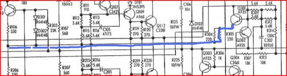
Have you looked at/measured etc those parts I highlighted. D304 provides an "auxiliary" supply for the protection part of the circuit... whats the DC volts across C304 and 305... you are going to have to fault find on this.
If the output of the amp is around zero volts DC as measured on R124 and 224 then the problem lies elsewhere.
It's a very contrived circuit... what's is the voltage on this line ? it should be nearly the same as the negative rail. If not we are back to the area of those highlighted components again.
Attachments
I gotta say, that doesn;t look like any Peavey product I have ever seen, and I have run a Peavey authorized repair shop the last 25 years. That doesn;t alter your problem, of course.
Yes that isn't a Peavy product but rather a Gemini. Error or mistype on the OP's part.I gotta say, that doesn;t look like any Peavey product I have ever seen, and I have run a Peavey authorized repair shop the last 25 years. That doesn;t alter your problem, of course.
Yeah, another typo on my part. I have no idea why I called it a Peavey when it clearly is not! It is of course a Gemini PVX-125.
I have measured the voltages across the components you highlighted Mooly I will try to show readings below.
C303: PD = 3.01V
R319: PD = 2.16V,
PD/gnd from R319/C303 junction = 2.16V
PD/gnd from R319/C304 junction = 0.12V
R325: PD = 172mV
PD/gnd from R325/R319 junction = 172.4mV
PD/gnd from R325 = 0V
C305: PD = 210mV
PD/gnd from C305/R325 junction = 121mV
PD/gnd from C305/C306 junction = 94mV
You say this is an a power supply to drive the protection circuit, what would be a typical output of such a power supply circuit?
The potential difference of the line you have highlighted is -190mV with respect to ground.
What is the line you have highlighted?
Sorry, not notified of your posting 🙂
http://www.diyaudio.com/forums/forum-problems/148984-bugs-13.html
post #243 It's a real problem.
I'll look later 🙂
That line... a lot's happened since then 😉... it's a switched rail, when working it should be around the value of the main negative rail (as I remember... have to look at it all again).
What's on the collector and emitter ? when you power up.
Just had another look at the circuit.
Q301 is used to switch the negative rail to the front end.
Collector goes to negative rail so should have -60volts or so (whatever the negative rail is). That should also be on the emitter.
Those voltages you gave look wrong 🙂
Is D304 open circuit ? You should have around 60 volts DC on the cathode (which is also the voltage across C304).
If it is faulty I would replace C303 and C304 and check the 1.5K (R325) is OK.
- Status
- Not open for further replies.
- Home
- Amplifiers
- Solid State
- noob with a perplexing problem.