I have this PS Audio 200c amplifier, which seems to function and sound fine.
However... When I removed the bottom panel , I got a look at the underside of the main amplfier boards. There is a "hot spot" on one board (looks darkened due to heat) about the size of a dime or smaller. Whats going on there is a trace on the board has somehow worked its way out of the board. So theres about 5mm worth of trace exposed, along with the solder point which has pulled away along with the trace.
The connections are still intact naturally, but now I wonder, is this something that can be fixed? I also noticed on this board, that a few solder points have some "frosty" looking corrosion on them. Interestingly all of this is on one board but the other one looks pretty clean.
any advise would be appreciated.
Thank You
Local hot spot has boiled off the glue which holds the track to the board.
Replace the hanging trace with a short length of copper wire, clean up, superglue back in place, then coat with conformal coating.
Run over the 'frosty' joints with a hot iron and some quality solder, clean and recoat the board.
Good for another twenty years....
Replace the hanging trace with a short length of copper wire, clean up, superglue back in place, then coat with conformal coating.
Run over the 'frosty' joints with a hot iron and some quality solder, clean and recoat the board.
Good for another twenty years....
Member
Joined 2009
Paid Member
I believe it can be fixed, but you need somebody skilled in this kind of thing. I remember Anatech telling me he has done this kind of thing before to a professional standard - try ping him a PM for some advice.
Frost sounds like solder flux wasn't cleaned off properly.
Frost sounds like solder flux wasn't cleaned off properly.
A picture would help us see 🙂
If the board is carbonised, then that should really be cut (drilled) out. Once a board is in that state it can become conductive and the whole thing gets worse. You can fill the space with an epoxy resin etc and hard wire across.
Components/leads/wires that have crusty solder can be a problem to re-tin well.
Used to see these issues all the time in the TV trade... you could also get special high melting point solder...
Well this sounds promising then, which is a bit of a relief really.
Bigun, your call on the flux is spot on. I noticed plenty of this on both boards.
I'll most likely contact Cullen, as he is the PS Audio go-to guy it seems, and I'm not to experienced with small stuff like this (and these board are no longer available...).
However, shipping this amp is going to be a pain (70lbs unpacked). I might alternately check with the guys at audiolab in Cambridge,MA since I could actually drop it off there. Any feedback on repair shops in the MA/NewEngland area?
Thanks for the replys
A picture would help us see 🙂
If the board is carbonised, then that should really be cut (drilled) out. Once a board is in that state it can become conductive and the whole thing gets worse. You can fill the space with an epoxy resin etc and hard wire across.
Components/leads/wires that have crusty solder can be a problem to re-tin well.
Used to see these issues all the time in the TV trade... you could also get special high melting point solder...
Just to follow up, I took this to an experienced tech who basically agreed with you. However, modifying the actual board for him would be huge $$$. Of course this is the DIY community, and I've got some really useful info, but modifying the board is beyond my personal reach.
The good news is that it works perfectly fine now, and the transformer that I pulled to have serviced (vacuum dip/cure etc) appears to be successful in getting rid of the transformer hum
The tech is going to clean it up and re-enforce the trace. Basically the trouble seems to be in actual design itself. There are a pair of transistors in the center of this location on each channel. It would seem, as pointed out to me, that it would have been far better for these to be heat-sinked in the original design, which neither are. He's going to try to find a light-weight sink to dissipate the heat (Suggestions? clip ons?...)
I'll try to update with a pic if interested. (best i can do atm)
Attachments
Last edited:
From the piccy they look like TO220 style packages so something like this,
EG & G VACTEC|576802B00000|HEATSINK,WARTHTO220CLIP | CPC
or this which needs a nut/bolt,
EG & G VACTEC|274-1AV|HEATSINK,WARTHTO220 | CPC
so you will have to trawl local suppliers.
Depending on what those devices are used as there are two points to watch,
1. The tab will not be isolated, so it mustn't touch anything else.
2. And more unlikely... if the tab were say a collector on a VAS stage then the heatsink may add stray capacitance and "alter" the HF characteristics, or "radiate" the signal there to nearby sensitive stages.
Almost certainly not an issue that last one 🙂
Anatech is the man...others know a lot too...but anatech
has made the job to fix things for years long...he is the man...ask anatech what to do, he may confirm some suggestions...if not, follow anatech advice.
And learn the best Anatech advice:
- "just because you can do, this does not means you should do!"
regards,
Carlos
has made the job to fix things for years long...he is the man...ask anatech what to do, he may confirm some suggestions...if not, follow anatech advice.
And learn the best Anatech advice:
- "just because you can do, this does not means you should do!"
regards,
Carlos
.....2. And more unlikely... if the tab were say a collector on a VAS stage then the heatsink may add stray capacitance and "alter" the HF characteristics, or "radiate" the signal there to nearby sensitive stages.
Almost certainly not an issue that last one 🙂
Thanks for the info Mooly. I'm not quite sure about #2, the tabs are free to the air with no contact. The amp is still in the shop until I can pick it up next week, so I can't tell you what ones they are from this schematic.
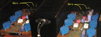
This is a good thread ( SQLGuy ) I searched awhile back and just revisited. Those transistors are actually sink'd in this picture.
http://www.diyaudio.com/forums/solid-state/136822-ps-audio-200c-repair-upgrade.html I re-attached pics to this thread (mines on the left, SQLGuy's is the middle showing heat sinks)
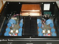
My amp looks a bit different, ( see attached #0209 )and is also older. Maybe those transistors where actually replaced once before and the tech never replaced the heat sinks, who knows
@Carlos: That advice --- "just because you can do, this does not means you should do!" I should have used before I bought the amp 😀
High-Insight is 20/20 though. But I do like the sound of this amp - allot.
I guess I'll get a few more years out of it until that channel goes. Is there a way to get a limited run on circuit boards that isn't outrageously expensive? Theres got to be a way, this board doesn't look that complex. I might even be able to get it fully laid out for free.
Attachments

Last edited:
There are quite a few resources for PCB repair. Circuit board rework and repair - BGA component rework and repair is one such place. I learned quite a bit about repairing PCB's and have successfully brought back from the dead many boards that rightfully should have been trashed.
I bought a through hole repair kit that has helped to repair traces where the pad has been damaged. it comes with a small carbide cutter used to enlarge the hole. then a ferrule is installed and swedged into place. works great.
I have fixed some boards that have had large holes burned in them. you have to grind away all the black, burnt parts of the board. the carbonized spots as they are conductive. I then take old PCB boards that i have removed the copper traces from and grind them into a powder that I mix with Epoxy into a paste. and fill in the hole. once hardened I use a dremel tool to smooth out the surface and clear away any epoxy near solder pads etc. This has worked well for several boards now. Not sure how they will stand up with the test of time but figuring a PCB is just epoxy and fiberglass, this repair should be pretty good.
For traces that have pulled loose. I use a bit of epoxy under the trace.just enough to stick the trace down. then a little bit applied to the top of the trace to act as a coating and to help continue to hold the trace down. If the component about that spot on the board is a resistor that stands off the board. some sort of support will help. either bending the leg on the top side of the board or a dab of epoxy or silicone or some other type of stand off to help hold the part from wiggling.
Some MFG put parts heat producing parts too close to the board. if i see a spot on the board getting "Tan" I will replace the part and mount it so it has at least a little bit of clearance and airflow around it. a little bit can go a long way.
For example, from the circuit rework website. here is a tutorial on repairing a lifted PCB trace. 4.1.1 Lifted Conductor Repair, Epoxy Seal Method
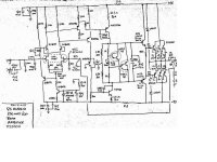
Looks like the TIP48 and MJE5930 to me that have the clip on heatsinks.
The drivers shown in the circuit have ferrite beads on the base and these are visible in the pictures as the ones on the main heatsink.
See how hot they run ? You could measure the volts across the 12.1 ohm resistor, calculate the current and multiply by 75 volts to get the power disipation under quiescent conditions... which would be useful to know.
For example, from the circuit rework website. here is a tutorial on repairing a lifted PCB trace. 4.1.1 Lifted Conductor Repair, Epoxy Seal Method
Thank you, nice info and links. I think what I'm going to need to do is buy some simple diy electronic kit(s) for practice if I'm ever going to dive into this myself. Mainly due to my lack of soldering skills🙁. The transistor(s) will definitely need to be pulled, as the trace is a connector to it ------o
So you can imagine that the connecting trace, being pulled away, is taking the transistor with it ( the solder point has pulled off the board too, but remains in full contact. When I get the amp back, I'll take a picture of the spot so people know what it looks like exactly, but it sounds like people pretty much know what this is all about anyway.
Good thing is that, for now, it's being cleaned up, reinforced, and I believe adding the heat sinks will help...for awhile...
Looks like the TIP48 and MJE5930 to me that have the clip on heatsinks.
The drivers shown in the circuit have ferrite beads on the base and these are visible in the pictures as the ones on the main heatsink.
See how hot they run ? You could measure the volts across the 12.1 ohm resistor, calculate the current and multiply by 75 volts to get the power disipation under quiescent conditions... which would be useful to know.
Why the heck do you think no one put heat sinks on these at least? Even still, having them situated on the board this way seems flawed. This isn't the first board I've seen on the 200c with this sort of damage in this area.
Why the heck do you think no one put heat sinks on these at least? Even still, having them situated on the board this way seems flawed. This isn't the first board I've seen on the 200c with this sort of damage in this area.
Can't answer that 🙂
Were they added later in production as a problem appeared, or as you suspect has it been worked on before and they haven't been replaced.
I've seen plenty of gear that has parts that run so hot they are on the point of unsoldering themselves... a certain famous best brand TV had two standup resistors that did this and burnt and huge hole in the pcb. Official mod... clean/repair if possible and use special high melting point solder. They are faults waiting to happen but products still get turned out that way.
- Status
- Not open for further replies.
- Home
- Amplifiers
- Solid State
- Board goin bad