Hallo,
I am a newbie in diy elektronics, but I want to make a lm1875 amplifier. I've found several pcb layouts for the gainclone circuit, but they aren't in black and white, so I can't use them with out modification.
Does anyone has a pcb layout? It would make it a lot easier for me.
ps. I've found this one: http://i239.photobucket.com/albums/ff150/sneih/NewLayout1875.jpg but it's not as minimalistic as the gainclone circuit. I don't like the elco in the signal pad. (I don't know what the effect will be on the audio quality)
Regards,
Stefan
make sure you adopt an AC coupled schematic that has RF filter on the input and Zobel load at the output.
Hallo,
I am a newbie in diy elektronics, but I want to make a lm1875 amplifier. I've found several pcb layouts for the gainclone circuit, but they aren't in black and white, so I can't use them with out modification.
Does anyone has a pcb layout? It would make it a lot easier for me.
ps. I've found this one: http://i239.photobucket.com/albums/ff150/sneih/NewLayout1875.jpg but it's not as minimalistic as the gainclone circuit. I don't like the elco in the signal pad. (I don't know what the effect will be on the audio quality)
Regards,
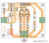
It look like this circuit'PCB, Lots of guys do it . It was said very good.
You can also try 2, 3circuit,It was said the third is the best.The second is better than the firist circuit. I use the samplest.
Attachments
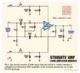
look at this http://www.diyaudio.com/forums/chip...-gainclone-hifi-lm1875-amplifier-board.html,I think it's the same,he explain it very claer,Sorry for my poor English,maybe you don't unerstand what i said🙁.
and the otrer two circuit without pcb.
and the otrer two circuit without pcb.
Attachments
Last edited:
Thank you very much!
No problem with your english 91art, (I'm also not a native speaker myself)
I'm gonna use the pcb from ratza.
No problem with your english 91art, (I'm also not a native speaker myself)
I'm gonna use the pcb from ratza.
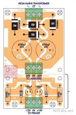
Ratza's PCB needs the power ground to pass up between the decoupling capacitors. The long Power ground traces that tie in the caps adds too much inductance to let the little 100nF caps do any good.
The signal ground should be separate from the power ground.
Leave a pair of pads to connect the signal ground to the ground terminal by a copper link wire or a 10r resistor and a pair of inverse parallel diodes.
Look at the Power ground and the Signal ground in post4 middle pic for ideas.
The signal ground should be separate from the power ground.
Leave a pair of pads to connect the signal ground to the ground terminal by a copper link wire or a 10r resistor and a pair of inverse parallel diodes.
Look at the Power ground and the Signal ground in post4 middle pic for ideas.
Last edited:
AndrewT, you're right regarding traces' inductances. Yet the amp is mute. I just wanted a very compact board in THD technology.
See if these suit your needs.
Ratza could you post schematic for this project?
Regards Aleš
mravlca,
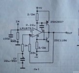
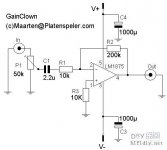
The schematic is from the lm1875 datasheet, the one with the symmetric power supply.
I noticed that, but I got confused by those two capacitors that have value 2.2uF. I understand that one is input cap but then the other one should be 22uF if I refer to the datasheet scheme.
Regards Aleš
@mravlca hmm.. I didn't look very good. It's a little bit different from the circuit in the datasheet
@91art: Do you have this pcb layout in black and white? So I can print them immediately on a transparent sheet (for etching).
@91art: Do you have this pcb layout in black and white? So I can print them immediately on a transparent sheet (for etching).
the schematic is here:
http://www.diyaudio.com/forums/atta...20080408_af07e42a6d060385c3abzbfg5dlygsgg.jpg
It was already posted in this thread!
http://www.diyaudio.com/forums/atta...20080408_af07e42a6d060385c3abzbfg5dlygsgg.jpg
It was already posted in this thread!
I myself would like to have PCB artwork ready for use for the amp board and P/S for these that were shown by 91art.
Anyone have them??
Prefer in PDF if available.
Thanx: E-C
Anyone have them??
Prefer in PDF if available.
Thanx: E-C
I myself would like to have PCB artwork ready for use for the amp board and P/S for these that were shown by 91art.
Anyone have them??
Prefer in PDF if available.
Thanx: E-C
It's the same compare with pdf,use photoshop change the size you want it will be work. it was draw by my friend,i didn't have Original image, in fact it fit
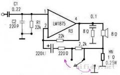
Beginners, most of us buid it like this taht use the elements directly connected.
Note:
1.Signal line to use shielded cable
2.Back capacitance and signal lines do not even connected to the point
3.Transformer not less than 60W
4.Components as much as possible close to the IC,It's very important.
Attachments

It requires good welding technology,Otherwise,you need anoter two 0.1UF CBB capacitors parallel to the 1000UF retreat capacitors.
Ratza's PCB needs the power ground to pass up between the decoupling capacitors. The long Power ground traces that tie in the caps adds too much inductance to let the little 100nF caps do any good.
The signal ground should be separate from the power ground.
Leave a pair of pads to connect the signal ground to the ground terminal by a copper link wire or a 10r resistor and a pair of inverse parallel diodes.
Look at the Power ground and the Signal ground in post4 middle pic for ideas.
Well, would that make a difference I can hear?
Does anyone have a pcb for the circuit in the ns lm1875 datasheet with shorter power ground traces?
Ratza's PCB is so small that I doubt that the lenght of gnd trace has any influence to the inductance and I think that you won't hear difference if you as AndrewT suggested.Well, would that make a difference I can hear?
Does anyone have a pcb for the circuit in the ns lm1875 datasheet with shorter power ground traces?
Regards Aleš
You got it right guys, the schematic is the one from the datasheet. I used the same values both in feedback and input to see how the circuit behaves. Well, it plays very good, both in speakers and in the dummy load 🙂 Everybody is free to put whatever they want, including short circuiting them, although I don't recommend it.
AndrewT's suggestions are always welcome. It's very hard to hear a difference of 5mm trace length, even if for the IC might be a difference. For those who think that the PCB is big, the size is 39x27mm (around 1.5x1.1 inches). The length of the ground is around 25mm and the parasitic inductance is no more than 0.5nH for each capacitor so it's not that big for audio.
So, even if I designed and built this amp just for fun, in the end it proved to be quite good and I think I'm going to use it as the "reserve" amplifier. It needs a case 😀
- Status
- Not open for further replies.
- Home
- Amplifiers
- Chip Amps
- lm1875 pcb layout for gainclone.