Hi All
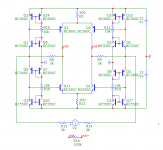
Here is a concept design that I have simulated for a high performance descrete differential current to voltage converter for the differential current output DAC's (and possibly for other similar applications).
The idea was to build a quality DAC based on PCM1794 or AD1955's but I wanted to do my own analog section. I had been playing with the idea, of a push pull common base, I-V input for quite a while but I couldn't quite make it properly differential until recently, so i though i would share what i have done.
I do have to thank Jocko's for the input transistor biasing idea.
I hope you enjoy.
Tim
Attachments
Hi,
interesting and yet simple.
No capacitors, anywhere! Is this a measure of it's "goodness"?
Have you tried a breadboard version yet?
interesting and yet simple.
No capacitors, anywhere! Is this a measure of it's "goodness"?
Have you tried a breadboard version yet?
Hi Andrew
I haven't breadboarded it yet, it has just gone from my imagination to the simulation. But I will let you know when it is done.
I don't know if it is a measure of its goodness but since the circuit is a 2 stage design it is stable without compensation capacitors and the input and output can be DC coupled.
Though I will be needing caps to roll off its frequency response because it is -3dB at about 20MHz (according to sim).
Also (in the simulation) it has vanishingly low distortion (22ppb @ 1khz, 0.5mA peak), but I think that is from the sim using perfectly matched parts.
Cheers
Tim
Hi,
interesting and yet simple.
No capacitors, anywhere! Is this a measure of it's "goodness"?
Have you tried a breadboard version yet?
Your design looks interesting , and I think your choise of DAC chip is also well thought. Just now there is a lot of hype around the ESS DACs, which is very simple to implement, as it has both ARSC and SPDIF reciever as well as a digital filter on board.
Will you feed the 1794A from a sample rate converter?
I hope you´ve considered preceeding with discrete design for your output amplifier. If you did, feel free to be inspired by our work here http://www.diyaudio.com/forums/showthread.php?t=138230
I recommend using the shunts, they are very low noise and low output impedance.
, and I think your choise of DAC chip is also well thought. Just now there is a lot of hype around the ESS DACs, which is very simple to implement, as it has both ARSC and SPDIF reciever as well as a digital filter on board.Will you feed the 1794A from a sample rate converter?
I hope you´ve considered preceeding with discrete design for your output amplifier. If you did, feel free to be inspired by our work here http://www.diyaudio.com/forums/showthread.php?t=138230
I recommend using the shunts, they are very low noise and low output impedance.
How do you plan to deal with the 6.2ma of offset of the pcm1794 ?
You're going to need very tight matching of the bjt for it to work. I simulated it quickly with bc547c and bc557c. Simply replacing one bjt by a b grade gives completly messed up sinewaves.
You're going to need very tight matching of the bjt for it to work. I simulated it quickly with bc547c and bc557c. Simply replacing one bjt by a b grade gives completly messed up sinewaves.
Hi Kurt
My choice of DAC comes from availability and the requirement for it to be a differential current output. I have looked at the ESS's but they seem difficult to buy and to learn about
I am new to DIY DAC, I am more of an amp guy so this is an exercise to try my ideas in current to voltage converters as well as building a great digital source.
I am not sure what digital receiver would be the best the application note uses the CS8414 but I am sure there is better out there. Maybe somebody could make some suggestions, I think my requirements would be to support up to 192kS/s.
There seems to be a lot of debate about the type of regulator and I haven't decided which I will use, maybe a series regulator followed by a shunt regulator, I am not sure yet.
Thanks for your comments
Tim
My choice of DAC comes from availability and the requirement for it to be a differential current output. I have looked at the ESS's but they seem difficult to buy and to learn about
I am new to DIY DAC, I am more of an amp guy so this is an exercise to try my ideas in current to voltage converters as well as building a great digital source.
I am not sure what digital receiver would be the best the application note uses the CS8414 but I am sure there is better out there. Maybe somebody could make some suggestions, I think my requirements would be to support up to 192kS/s.
There seems to be a lot of debate about the type of regulator and I haven't decided which I will use, maybe a series regulator followed by a shunt regulator, I am not sure yet.
Your design looks interesting
Will you feed the 1794A from a sample rate converter?
I hope you´ve considered preceeding with discrete design for your output amplifier. If you did, feel free to be inspired by our work here http://www.diyaudio.com/forums/showthread.php?t=138230
I recommend using the shunts, they are very low noise and low output impedance.
Thanks for your comments
Tim
Hi
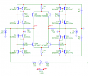
These were some very good points and they had me back at the simulator for a while.
Since I was a noob at DAC's I overlooked the current offset in the datasheet.
After a some playing on the sim I came up with a couple of options:
1 - keep the circuit biased symmetrically which but the 6.2mA offset would cause a large common mode DC offset, which can be removed with capacitors, but the supply rails had to be increased so the output doesn't clip.
2 - Asymmetrically bias the input current mirrors (maybe with a trimpot) so the 6.2mA is cancelled out.
I decided for the moment to use option 2 which I have attached. (BTW I wasn't sure if the offset current is sinking or sourcing. I guessed sinking since the current is negative in the datasheet but the circuit is easy to modify if the offset current is sourced)
BJT matching can be an issue. I did try what you did and changed the grade of various transistors too see the effect.
Changing the grade of the output pairs increased the output distortion to about 0.001% so not really an issue.
Changing one of the devices in a current mirror made a big difference in the wave shape, and this is what I think you saw, but if both devices were made the same in the current mirror then the problem went away.
I did try putting degeneration resistors on all of the emitters but they didn't seem to help much.
I think as a rule the current mirrors should be matched as well as Q3/Q4 and Q11/Q12.
And finally there is the THAT3xx matched transistor packages, these would be perfect except they are only suitable for IEmax of 10mA which is not enough.
Thanks for your questions
Tim
These were some very good points and they had me back at the simulator for a while.
Since I was a noob at DAC's I overlooked the current offset in the datasheet.
After a some playing on the sim I came up with a couple of options:
1 - keep the circuit biased symmetrically which but the 6.2mA offset would cause a large common mode DC offset, which can be removed with capacitors, but the supply rails had to be increased so the output doesn't clip.
2 - Asymmetrically bias the input current mirrors (maybe with a trimpot) so the 6.2mA is cancelled out.
I decided for the moment to use option 2 which I have attached. (BTW I wasn't sure if the offset current is sinking or sourcing. I guessed sinking since the current is negative in the datasheet but the circuit is easy to modify if the offset current is sourced)
BJT matching can be an issue. I did try what you did and changed the grade of various transistors too see the effect.
Changing the grade of the output pairs increased the output distortion to about 0.001% so not really an issue.
Changing one of the devices in a current mirror made a big difference in the wave shape, and this is what I think you saw, but if both devices were made the same in the current mirror then the problem went away.
I did try putting degeneration resistors on all of the emitters but they didn't seem to help much.
I think as a rule the current mirrors should be matched as well as Q3/Q4 and Q11/Q12.
And finally there is the THAT3xx matched transistor packages, these would be perfect except they are only suitable for IEmax of 10mA which is not enough.
How do you plan to deal with the 6.2ma of offset of the pcm1794 ?
You're going to need very tight matching of the bjt for it to work. I simulated it quickly with bc547c and bc557c. Simply replacing one bjt by a b grade gives completly messed up sinewaves.
Thanks for your questions
Tim
Attachments
Hi
These were some very good points and they had me back at the simulator for a while.
Since I was a noob at DAC's I overlooked the current offset in the datasheet.
After a some playing on the sim I came up with a couple of options:
1 - keep the circuit biased symmetrically which but the 6.2mA offset would cause a large common mode DC offset, which can be removed with capacitors, but the supply rails had to be increased so the output doesn't clip.
2 - Asymmetrically bias the input current mirrors (maybe with a trimpot) so the 6.2mA is cancelled out.
I decided for the moment to use option 2 which I have attached. (BTW I wasn't sure if the offset current is sinking or sourcing. I guessed sinking since the current is negative in the datasheet but the circuit is easy to modify if the offset current is sourced)
BJT matching can be an issue. I did try what you did and changed the grade of various transistors too see the effect.
Changing the grade of the output pairs increased the output distortion to about 0.001% so not really an issue.
Changing one of the devices in a current mirror made a big difference in the wave shape, and this is what I think you saw, but if both devices were made the same in the current mirror then the problem went away.
I did try putting degeneration resistors on all of the emitters but they didn't seem to help much.
I think as a rule the current mirrors should be matched as well as Q3/Q4 and Q11/Q12.
And finally there is the THAT3xx matched transistor packages, these would be perfect except they are only suitable for IEmax of 10mA which is not enough.
Thanks for your questions
Tim
Hi Tim,
Have you considered a servo taking the output CM offset and driving a compensation DC current into the input? An opamp based servo as often used in pre- or power amps? A proven technology, it would do away with adjustments and you can keep the current mirrors equally biased, which is necessary to avoid all kind of drift problems (which you won't see on the sim of course).
Jan Didden
No problem. I'm actually very interested by your design. I decided to return to the opa1632 for my DAC, after failing to get a discrete conveyor design to work properly. I might try an alternate output stage one day 😉
I picked the PCM1798 rather than the 1794. The 1794 outputs are very hot, which isn't without problems for a discrete design with to92 devices. The digital filter isn't as good though... trade offs.
The easy way is to add in your sim a I/V with an opamp. The output of the opamp must be negative for your current source to be correct (see the application design in the datasheet for more details).
I picked the PCM1798 rather than the 1794. The 1794 outputs are very hot, which isn't without problems for a discrete design with to92 devices. The digital filter isn't as good though... trade offs.
It always confuse me too... 😛BTW I wasn't sure if the offset current is sinking or sourcing. I guessed sinking since the current is negative in the datasheet but the circuit is easy to modify if the offset current is sourced
The easy way is to add in your sim a I/V with an opamp. The output of the opamp must be negative for your current source to be correct (see the application design in the datasheet for more details).
I picked the PCM1798 rather than the 1794. The 1794 outputs are very hot, which isn't without problems for a discrete design with to92 devices. The digital filter isn't as good though... trade offs.
Can you not increase the Iref resistor (10k to ground by default) to lower the output current? I'm sure I read that somewhere. Kind of like an analogue volume control...
TimS, temperature of Q1 Q9(and other pairs) will be different becouse Q9 dissipate less power then Q9 so the voltage at the input stage will be different from zero (20-40mv), so it should cascode Q1, such as I did in this old design http://diyaudio.org.ua/blog.php?u=2&b=6
In addition, the discrete output for the DS DACs will be a bad idea because it would occupy too much space on the PCB and therefore catch too much interference.
1794 Offset removes simply by adding 2.4k resistors from -15v power supply to 1794 outputs.
In addition, the discrete output for the DS DACs will be a bad idea because it would occupy too much space on the PCB and therefore catch too much interference.
1794 Offset removes simply by adding 2.4k resistors from -15v power supply to 1794 outputs.
- Status
- Not open for further replies.
- Home
- Source & Line
- Digital Line Level
- Descrete Differential Current to Voltage Converter