we just finished outlining the volume attenuator design (after 2 years), which grew to be a very interesting one and Im goin to utilise it on the same PCB . I am too interested, what do you think of buffer IC-s like buf634 and LME49600 ? Are those considered 'opamp sound' contributors as well ?
Yes!
They are dead dull, even if provided with state of the art PSU´s!
Please don´t use our DAC construction in conjunction with things like that.
You ought to wait for the more simple op-amp based DAC upcomming, this will surely suit you a lot better, and integrate much more smoothely with your system.
This DAC project is only suitable for nerds considering every stage in the most painstaking way, and being well aware of any components contribution to the final sound of their system.

Will you consider building the DAC??
No, too much smd and no tubes. 😀
I was very curious though for the schematics as you said you were designing a "state of the art DAC". Still, I would love to hear it.
Jeroen
No, too much smd and no tubes. 😀
I was very curious though for the schematics as you said you were designing a "state of the art DAC". Still, I would love to hear it.
Jeroen
Well right you are, there are very few tubes in the design, and indeed there is a lot of SMD components.
If you want to listen to it, welcome you shall be, but warned you must be, there are even fewer tubes in the rest of the set-ups used for development.

Last edited:
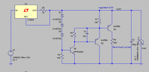
I fully understand your doubt about this. Anyway.... PSpice simulations has shown an output impedance of approx 7milliohm from DC to 20MHz.
Real life measurements has shown something around 12-13milliohm from DC to 10MHz.
...
T´he shunt itself isn't any secret... It has been used by various designers. But in combination with a true current source, we have achieved extreme PSRR in the regulator.
PSpice simulations say around 160-180dB. I have not been able to measure it yet, but my guess real life is around 120dB.
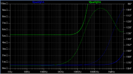
Hi, and thanks for posting the schematics. I tried simulating the circuit attached. I had to guess T313 and the resistor that sets the current on the lt1085. I chose a load of about 60mA and a shunt current of around 60mA, not to be too extreme.
The second plot shows the output impedance, and third shows psrr. Dotted lines are phase. The green line is your circuit, the blue line is how I would have changed it.
The psrr is decent. The Zout values you claimed are not quite in tune even with simulation.
If I made a mistake in recreating your circuit please do advise.
Attachments

schematic has an error
In your schematic "Analog Stage.pdf" you have connected the negative shunt for each channel into the servo circuit of each channel. There is no source for the negative rail.
for example, you need to connect emitter of T315 to pin 4 of the LF411 instead of pin 6.
In your schematic "Analog Stage.pdf" you have connected the negative shunt for each channel into the servo circuit of each channel. There is no source for the negative rail.
for example, you need to connect emitter of T315 to pin 4 of the LF411 instead of pin 6.
The schematic for the SPDIF input doesn't show the isolation transformer that is visible in the earlier pictures in the thread.
This allows the possibility of a ground loop through the RCA cable to the digital source power supply. That can introduce noise into the DAC PCB.
Also the CS8416 cannot tolerate signal on the RXP inputs greater than the VL. That little Zener diode may not be good enough.
Study the pages 27 and 49 in the Cirrus Logic CS8416 data sheet.
The schematic for the SPDIF input doesn't show the isolation transformer that is visible in the earlier pictures in the thread.
This allows the possibility of a ground loop through the RCA cable to the digital source power supply. That can introduce noise into the DAC PCB.
Also the CS8416 cannot tolerate signal on the RXP inputs greater than the VL. That little Zener diode may not be good enough.
Study the pages 27 and 49 in the Cirrus Logic CS8416 data sheet.
There has never been any isolation transformer in the input of the DAC, as the DAC is intended for use in hifi systems. If connected to a computer or like, you should either use optical or electrical isolation.
@ikoflexer.
Why did you put 220µF in the output of the regulator.
This is not present on the schematics.
Our simulations of the circuit, says what we already told you.
Why did you put 220µF in the output of the regulator.
This is not present on the schematics.
Our simulations of the circuit, says what we already told you.
Well! Can´t seem to edit the former answer, but you also added a 1 Ohm resistor named R6 in your schematics, which isn´t in the original. I think what you see on your simulations are an oscilating circuit out of control, because of the load resulting from these two components.
The shunt is not decoupled in anyway, it supplies the amp directly, which is the basic idea of the shunt. It was chosen because it was possible to avoid any electrolytic caps in or near the amp. The only caps the amp has to wrestle, are the ones in the post filtering, which aren´t even placed in the signalpath. The cap tuning the cut of frequency in the DC servo, can in our opinion, not be considere as a part of the signalpath, as it is not active above a few milli HZ, and in reality is a part of a subsonic feedback loop. It tends to overshoot even temperature changes, so it is really slow.
The shunt is not decoupled in anyway, it supplies the amp directly, which is the basic idea of the shunt. It was chosen because it was possible to avoid any electrolytic caps in or near the amp. The only caps the amp has to wrestle, are the ones in the post filtering, which aren´t even placed in the signalpath. The cap tuning the cut of frequency in the DC servo, can in our opinion, not be considere as a part of the signalpath, as it is not active above a few milli HZ, and in reality is a part of a subsonic feedback loop. It tends to overshoot even temperature changes, so it is really slow.
In your schematic "Analog Stage.pdf" you have connected the negative shunt for each channel into the servo circuit of each channel. There is no source for the negative rail.
for example, you need to connect emitter of T315 to pin 4 of the LF411 instead of pin 6.
Thanks for the info...
As we did mention, the schematics is NOT finished yet, and that's really why I did not want to make them public yet.
But a few users have been very busy claiming this to be a commercial product, because we did not make the schematic public.
And now what??? Well.... As I did say, the schematic is NOT finished. It may contain errors, and that really the price every potential builder has to pay, for some other users "forcing" us to public these "almost done" schematics. Please send a big "Thanks 😡" to these users!!
I will correct the schematic as soon as I have the time for it.
The schematic for the SPDIF input doesn't show the isolation transformer that is visible in the earlier pictures in the thread.
This allows the possibility of a ground loop through the RCA cable to the digital source power supply. That can introduce noise into the DAC PCB.
Also the CS8416 cannot tolerate signal on the RXP inputs greater than the VL. That little Zener diode may not be good enough.
Study the pages 27 and 49 in the Cirrus Logic CS8416 data sheet.
We have NEVER used an isolation transformer. Don't know what picture you refer to. But not one of our DAC.
If you take a look at page 50 (Figure 1), you will see the tranformerless version of the input.
It is true that this may cause ground loops. Anyway..... we have NOT seen any such problems. On the other hand, the transformer will garuantee jitter levels way beyond the transforless version. And that really is why we do NOT use the transformer. We have done some testing on this, and there really is no doubt what to do, if you take the time to do the listening tests. Just to bad, that only so few people do. Most just claim to have done it 😉
I guess a lot of people will start investigating the DAC, and tell us things they believe to be non perfect. Just be aware, that we have already been there. We spend more than 4 years of tweaking on this design. Nothing has been accepted without listening tests. And what we have now, is what we believe to be the absolute best.
People who do not like this approach, may as well buy some sheap op amp based design.
Hi, and thanks for posting the schematics. I tried simulating the circuit attached. I had to guess T313 and the resistor that sets the current on the lt1085. I chose a load of about 60mA and a shunt current of around 60mA, not to be too extreme.
The second plot shows the output impedance, and third shows psrr. Dotted lines are phase. The green line is your circuit, the blue line is how I would have changed it.
The psrr is decent. The Zout values you claimed are not quite in tune even with simulation.
If I made a mistake in recreating your circuit please do advise.
As Kurt von Kubik pointed out, you have added a 220uF decoupling capacitor in the Shunt regulator. It seems like you have not spend time reading why we choose the shunt. Because it eliminates the need of this capacitor.
I do not know your background for analysing electronics designs. My background is as an electronics engineer and about 10 years for R&D experience.
If you have a degree in electronics engineering, you would know, NEVER to decouple a shunt regulator like this. It is supposed to into oscillation and even if it do not, the specificatios will be worse.
Also, Q1 in you schematic shoul NOT be a small signal transistor. Use a fast medium power transistor.
Also.... I do not know what CAE system you are using. I have always been using PSpice/OrCAD since that is what most engineering companys use here in Denmark.
If you do simulate the correct schematic in PSpice, you will actually get results very close to our measurements.
So the very short version. You claim that our specifications is incorrect, based on a simulation you did on the wrong schematic 😀
This really is the dark side of DIYAudio... 😛
Well!
Easy now folks!
@Ikoflexer!
We have tried out lots and lots of PSU´s in this project, incl. IC´s and decoupled very fast series regulators. The shunt only came about as an experiment, which theoretically should be better than the previous solutions (without any of us believing in it).
Without any prejudging, we implemented it in a very inoptimal way, but still it was very superior to our state of the art seriesregulators with quality decoupling caps.
And I guarantee that we tried out more caps than anyone will believe, and we found out, that they sound inferior all of them, even the best of them , just in different ways though.
The shunt in contrary is some kind of naked, pure and honest, and I´m sure, this would not be the case, if your simulations were valid, as even cheap caps do better measurements in most ways.
As already mentioned, you´ve changed the schematics for the shunts used, and in a way that completely ruins their performance. You should know that even 5 cm of quality leads will lead to performance imperfections of a shunt like this.
If not placed directly at the feet of the analog stage, a shunt like ours will cause problems at high frequencies, because of oscillation.
The fact is that the shunts output impedance is in the mOhm region from DC throughout the MHz region.
And now what??? Well.... As I did say, the schematic is NOT finished. It may contain errors, and that really the price every potential builder has to pay, for some other users "forcing" us to public these "almost done" schematics. Please send a big "Thanks 😡" to these users!!
You mean it is now my fault you posted an incorrect schematic? 😕
Oh dear....
You mean it is now my fault you posted an incorrect schematic? 😕
Oh dear....
What I say is:
The reason we did not want to upload the schematics yet, is that these are NOT finished yet.
But that did not keep people from accusing this to be a commercial project, because we did not upload the schematics.
To stop this, I agreed to upload the schematics as they were = not finished, even though I think it is wrong. I very clearly stated, that these were NOT finished, and that there were NO support on thse NOT finished schematics
And now people start talking about us uploading scehamtics that is not finished...
Please tell me.... What did we do wrong???
Please tell me.... What did we do wrong???
Main issue : you are arrogant. Look also at how you polluted the Buffalo thread.
Next : this thread is 8 months old. Walk the talk man!!
This is my last post here.
Well! Can´t seem to edit the former answer, but you also added a 1 Ohm resistor named R6 in your schematics, which isn´t in the original. I think what you see on your simulations are an oscilating circuit out of control, because of the load resulting from these two components.
The shunt is not decoupled in anyway, it supplies the amp directly, which is the basic idea of the shunt. It was chosen because it was possible to avoid any electrolytic caps in or near the amp. The only caps the amp has to wrestle, are the ones in the post filtering, which aren´t even placed in the signalpath. The cap tuning the cut of frequency in the DC servo, can in our opinion, not be considere as a part of the signalpath, as it is not active above a few milli HZ, and in reality is a part of a subsonic feedback loop. It tends to overshoot even temperature changes, so it is really slow.
The simulation was not oscillating. The 0R1 resistor I use for easy measuring the current through the shunt, it does not affect output impedance or anything else. Nor does the shunt capacitor. Removing them gives exactly the same results as I posted earlier.
As Kurt von Kubik pointed out, you have added a 220uF decoupling capacitor in the Shunt regulator. It seems like you have not spend time reading why we choose the shunt. Because it eliminates the need of this capacitor.
I do not know your background for analysing electronics designs. My background is as an electronics engineer and about 10 years for R&D experience.
If you have a degree in electronics engineering, you would know, NEVER to decouple a shunt regulator like this.
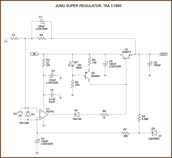
It seems that a few other people with a lot more credentials than me use a capacitor in that position, for instance the Jung super regulator?
Also, Q1 in you schematic shoul NOT be a small signal transistor. Use a fast medium power transistor.
Better tell me what you used in your simulations, I'll use the same. Unless it's a secret.
Also.... I do not know what CAE system you are using. I have always been using PSpice/OrCAD since that is what most engineering companys use here in Denmark.
If you do simulate the correct schematic in PSpice, you will actually get results very close to our measurements.
I use ltspice.
So the very short version. You claim that our specifications is incorrect, based on a simulation you did on the wrong schematic 😀
This really is the dark side of DIYAudio... 😛
That is not what I claim. What I said is that your claims are not in tune with my simulations.
The really dark side is not of diyaudio. The reason why I put even one minute in this is because there are people without the technical background who would accept your claims sight unseen. If your circuit is indeed what you say it is, you should be happy that I'm helping you get credibility. There is nothing more credible than independent tests of one's design.
- Status
- Not open for further replies.
- Home
- Source & Line
- Digital Line Level
- DAC project completed