Hi all,
It's been a while since I was on the forum!
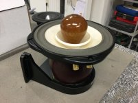
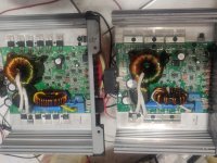
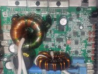
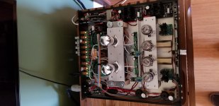
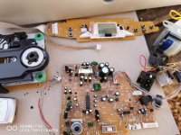
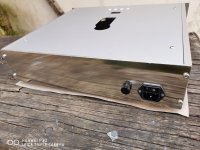
I have a QSC RMX 2450 amplifier that I bought with Channel 1 blown on ebay as a repair challenge. I finally got around to spending some time on it the other day, with mixed results:
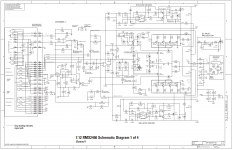
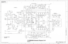
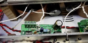
2x output transistors were blown on each side of CH1, as well as almost all the emitter resistors, one of the 22R B-E resistors on the negative side and the negative step driver FET as well. I replaced all the output transistors in the blown channel and the drivers for good measure, as well as the step driver FET. I was able to get the amplifier up and running and set the bias. Initial load tests looked good. I verified that the step drivers were working OK when the signal was big enough to need the higher-voltage rails. I connected a speaker and played some music, so far so good. However, a couple of gremlins remained.
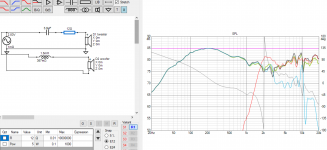
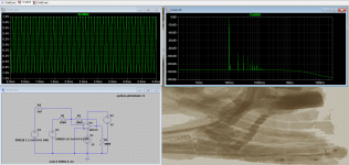
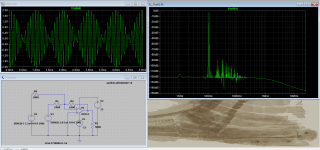
The first is that there is a slight thump in the speakers when it turns on. It is very slight, really not much, but it is noticeable. I thought the mute circuit was not being activated for long enough, however the manual says that approx 1 second muting is normal and I measured it as > 1second. Blue is negative rail, Yellow is one of the -15V opamp rails:
I am not sure why it still creates a bit of a thump, so I am open to some suggestions here.
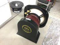
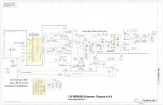
The second issue was the fan - it always runs, and it is a bit noisy. I assumed that the fan would be off until the amp warmed up enough to turn it on, but the circuit shows that it is always connected by at least 120R. I temporarily disconnected the cable from the Channel 2 PCBA to the AC PCBA and the fan ran a bit slower, so from this I know the optocoupler and the TIP31 are working OK - and the control circuitry on the Ch2 PCBA seemed to be working OK. With the amp off, the PTC on Ch1 reads 4-5 ohms higher than the one on Ch2 but other than that I could not find any anomalies with the circuit. It must just be a noisy fan, I will source a replacement.
However, while probing around - I inadvertently created a short. I use long, insulated HV probes which only have about 1mm of exposed metal on the tips when probing a live amplifier, but in their wisdom, QSC placed an uncovered via directly beneath the leg of D13 and while I was probing D13, I shorted its anode to ground with the tip of my probe. As far as I can tell from the schematic, this has the effect of collapsing the -15V opamp rail on Ch2. The effect of this was a little horrifying - the output emitter resistors on Ch1 all went up in smoke.
Now, before I pull it apart and replace the blown transistors again, I am trying to work out why this happened. I could believe that maybe some DC was fed to the driver stage when the negative opamp rail collapsed, but Ch2 seems to still be intact whereas Ch1 is now blown. Why? The opamps have separate sets of rails for each channel. The amplifier was in bridge mono mode at the time, so I am assuming that the signal was somehow coupled this way into Ch1, but again, why did Ch1 go up in smoke and Ch2 did not? I never set the current limiting on Ch1 after replacing the output transistors as I had trouble finding a 1200W 2-ohm load with which to do it, could this possibly be why? I measured the resistance across the current limiting trim pots and they are quite different between the 'good' Ch2 (540R and 570R) and the blown Ch1 (800R and 420R).
The thing is, I bought the amp with Ch1 blown, so I am just wondering if there is something else I have not considered that is leaving Ch1 vulnerable in some way. I'd welcome any advice or suggestions.
Any observations or advice would be quite welcome!


 .
. .
.


 Thought its about time.. I joined.