Hello friends, this is the story.
A good friend enjoyed this amplifier for about 10 years until one channel exploded. This also killed one of his favorite and expensive speakers. He asked me to take a look at it and try to fix it.
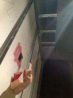
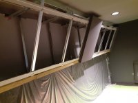
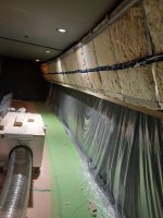
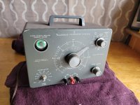
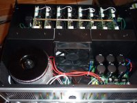
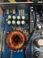
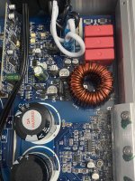
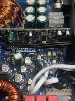
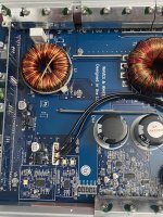
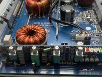
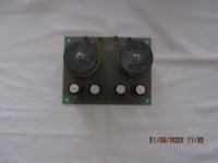
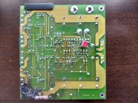
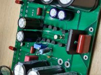
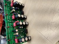
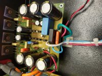
It has 2 identical small PCB's, one still works, the other can't be fixed because it caught fire. Literally. You may like to see the uploaded pictures.
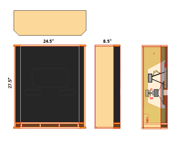
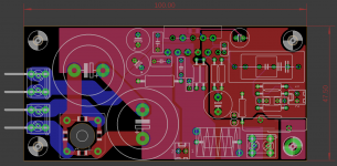
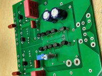
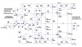
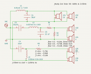
I made some research and could disassembly the dead channel PCB, and could entirely personally redraw the PCB and have it manufactured. The entire schematic could be deduced from the bare PCB. All parts measured. I am also uploading the schematic. The LTSpice working simulation file is also provided. I could recognize this circuit as some Goldmund variant, probably model 330. I tried making some of these variants from information gathered from this same site and I could make them work almost with no problem. The circuits I used were simpler, with Semelabs BUZ900/905 MOSFETS, and a simpler driver stage.
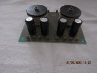
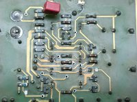
You can clearly see the different color of the PCB soldering mask. Lighter green for the old original amplifier, and darker green for my new, copied PCB. I bought all the parts from Mouser except for the lateral MOSFET's that I replaced for Exicon parts, obtained from Profusion, GB.
The problem: being the new PCB's identical to the originals, and being the original working board fairly stable and well behaved, the new replacement boards (I made 2 of them) is making me nuts 😱. The working voltage is +/- 60V and when my variac reaches the point for +/- 40V, I get a strong 22 MHz sine oscillation at the speaker output (no load), input shorted.
All kind of solutions I tried with no reasonable results at all. The only difference are the output MOSFETS. EXC10N20 and ECX10P20 in place of the originals Hitachi famous 2SK1058 / 2SJ162.
Ferrite bead on the gate terminal of each MOSFET, larger stopper gate resistors, small Zobel network placed across drain to gate of each MOSFET, compensation capacitors at previous VAS stage, heat sink connected to ground, etcetera.
Some strange things I detected by testing the original working amplifier.
In some way I think I could understand the reason, later on.
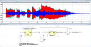
The working amplifier does not show quiescent current of the output MOSFET's. The offset balance trimpot does not show any kind of output DC change at the output when adjusted. The attached schematic shows this trimpot as R3 and R4. The output DC voltage with input shorted is about 2 mV or less. When applying input signal to this working amp, it shows no visible distortion, and delivers full 55 Vp-p sine wave from 5 to 50 KHz flat.
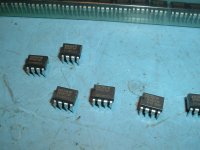
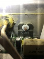
BTW, very hot Q1 and Q5 ! ... being small signal transistors TO-92. I believe that this could be the reason for no quiescent current at the output devices. I tried to raise Iq a little for a short time by changing R7 value from 330 to 430 Ohms. This should increase quiescent current to 130 mA per output device, that MOSFET's usually like. It worked, but Q1 and Q5 suffered. I returned to the original 330 Ohms value. But this amplifier and his twin worked for 10 years almost all day long, with excellent sound quality.
In the other hand, I don't know what else to do with my copy version. The Exicon MOSFET'S were ordered as matched units, 18 of each type N and P.
The only thing that make the oscillation stop was to place 2 x 100pF C3 and C4 capacitors, which I think is a huge value. The oscillation stopped but the output devices quickly raised their temperature, I don't understand why ! I thought I had solved the problem. 😕
Also, I lowered the feedback resistor R22 to 3K75 half its original value. No changes.😡 returned to riginal 7K5 Ohms value.
Please, could somebody help me think what can be done to make this amp work ? I would thank this help very much.
Finally: today I ordered 20 units 2SK1058/2SJ162 from Pacific Semiconductor in Canada, to avoid any fakes from other source. I have not too much hope because these are not matched units and these are too few pieces to get at least 2 matched pairs...
Thank you in advance !


.jpg")

.jpg")