Hello,
Long story short I suspect tilting back speakers about measly 10 degrees give or take would positively affect imaging.
This is a thread where it would be nice to collect some observations and experiences on tilting back loudspeakers, is it worth it.
Without further ado I'll explain an observation I had recently from VituixCAD simulation and I'd like to know better what you have experienced in terms of sound stage height and / or stability with and without tilt. If you have any comments regarding vertical early reflections and speaker tilt and height, crossovers, how we perceive the vertical reflections, what ever related.
There are attachments after the longish text explanation, scroll back and worth, it was bit hard to condense.
Observation from simulations:
Multiway speaker will have narrowing vertical response around crossover frequency on most typical two(+) way speakers between a tweeter and a woofer due to the drivers being not coincident but stacked one above the other, lobing. With symmetric crossover this narrowing is symmetric to vertical angles relative to listening axis meaning that above and below listening axis the frequency response is roughly similar 10 and -10, 20 and -20 etc.
On a typical listening situation a loudspeaker is positioned so that listening axis is about at ear height which is 90cm from floor in this example. Usually rooms (here in Finland at least) are about 2.5m tall and listening distance is 3m. Due to speaker and listeners ears being closer to floor than to ceiling angles towards first vertical specular reflections differ between floor and ceiling. On this example scenario the angles are roughly 30 degrees towards floor specular reflection and about 50 degrees towards ceiling. This means that with symmetric crossover frequency response towards these reflections are different. Also, floor being closer the path length through the floor is shorter than through the ceiling and this means less attenuation through floor reflection, which is louder of the two and arrives first to ear, right after direct sound making it probably dominant of the two.
Now the hypothesis from this observation regards to "vertical imaging" is that due to differing frequency responses that arrive to ear from high up and down below, and particularly nasty zigzag move right around crossover point which usually is right at the important vocal range and where ear is sensitive, affects perceived vertical image height/soundstage clarity/how would you call it. This is something I think I heard with quick listening test and would like to know what you think and hear.
Tilting speaker back some 10-15 degrees on this example scenario will make the response towards the first reflection points similar, no zig zag move and highs towards ceiling get boost and respectively attenuation towards floor. Same thing happens with my prototype speaker. I assume but don't know if its true, that if there is more sound through floor than through ceiling, and especially since the floor reflection arrives earlier, the perceived sound image height stays low. The zig zag move perhaps makes important vocal range image little bit hazy because there is more sound towards floor in general except around the crossover there is suddenly more sound to ceiling which perhaps pulls up this frequency zone a bit in perceived image, a confusing thing. When the two reflections are roughly balanced I assume sound image is stable at the speaker height, less confusing perceived vertical image. In addition if there was more highs through ceiling and more lows through floor would possibly elongate perceived vertical image some. If you know better or have links to studies, please comment!
This makes a lot of sense to me logically and I think I heard it but not so sure if its just bias
😀 Keep in mind direct sound frequency response also changes as speaker is tilted, but this could be adjusted if the scenario is planned in design phase. I'd be glad if you can share thoughts on it and especially if you have tried it. did vertical image or image in general get somehow sharper and perhaps even taller?
Here are some attachments for the text above.
This is made up sim with ideal drivers, its a two way box with 5" woofer and 1" tweeter, 20cm wide and 31cm tall, rather typical bookshelf speaker. The situation would be about the same for any loudspeaker that has a small tweeter and a woofer who are not coincident but stacked one above the other, perhaps 90% of all speakers out there, could be two or more ways, bookshelf or tower. Speaker with coincident tweeter and woofer (or a fullrange driver, or an array etc.) would have pretty much similar frequency response towards these reflections and perhaps there is not much difference. Perhaps this is partly the reason people like such speakers?
Drivers and baffle, responses made with mic at center for simplicity.


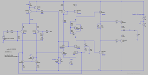
Here is the basic simple simulation setup. Arbitrary crossover point at 2500Hz, could be more or less doesn't matter, this is just some plausible crossover for such system.

Angle calculations, the room setup and simple right angle triangle calculator to get how much I need to increase tweeter Z coordinate with the Tilt angle in simulator. On the calculator B was set to driver c-c distance of 10cm and desired angle to alpha. This is not too accurate do it like so but accurate enough to zone in the tilt for listening experiment.


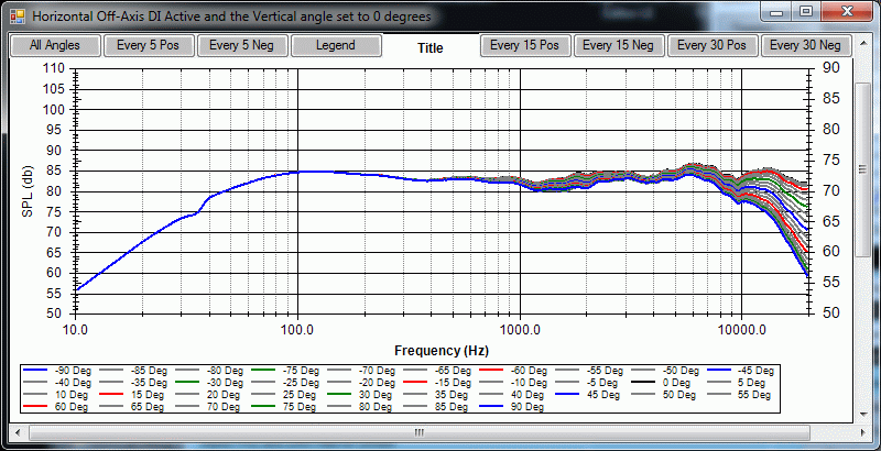
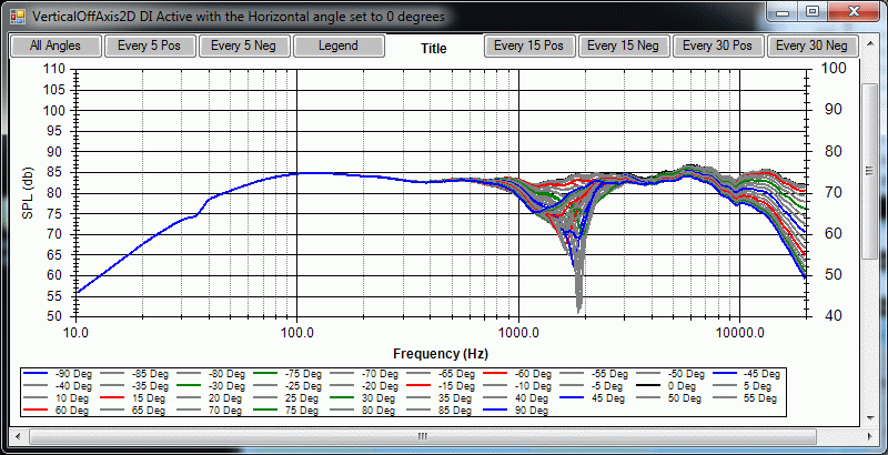
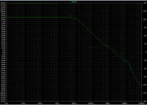
Here is the angles visible illustrating zig zag. Bottom graph shows -30 angle towards floor, direct sound and +50 angle towards ceiling. The zig zag happens roughly between 2-5kHz in this example, when ceiling reflection is relatively louder than floor reflection ( I think these graphs don't include attenuation due to path length ). Same graphs are also in power and DI window as light blue and light brown, these are default in VituixCAD so one doesn't have to setup the user defined angle if you are checking the stuff out in your project.

Now with small 10 degree tilt we can align the floor and ceiling reflection responses better so that dip due to lobing on both reflections happens roughly at same frequency. The hypothesis was that now both floor and ceiling reflections are about as loud through the whole frequency spectrum keeping the vertical image more stationary, stable. Alignment is not perfect but there is about no zig zag. 15 degrees would work fine as well but in the example listening axis response suffers already quite much. I don't know how bad this would be with your speaker, perhaps affects perceived sound or not.

Here is also 15 and 20 degree tilts. 20 degrees is too much in this case, zig zag is worse.


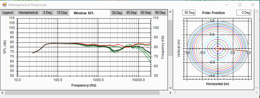
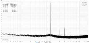
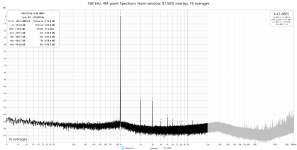
And here is completely another kind of system a three way with waveguide based on real measurements, not sure what kind of crossover slopes are, symmetric enough at least to make the zig zag. See the ER lines, light blue and brown. The first image is system adjusted before checking out this stuff, for basically power and DI and that kind of stuff. The second image shows that if I was to sacrifice some of the other lines and just adjust delay of the system to get tweeter back some and steer the nulls toward reflection angles the zig zag is gone. Not much of a sacrifice because the response can be adjusted for this new delay. Third image also tilts the waveguide little, now there is relatively more sound through ceiling on high frequencies than through floor, similar thing than perhaps a thick rug does as well. As frequency goes up more from above and less sound below listening axis. Here the 10 degree tilt works just fine.


I suspect your speakers and listening setup are suitable for the test. If you try tilting your speakers I suggest you to concentrate on vocals when listening for the effects of tilting but anything goes. What do you hear or is there any difference at all on sound image?
Here are some quick rough numbers to tilt your speaker roughly 10 degrees, put some Lego (a standard block is ~1cm high) or something else under front edge of your speaker. You could try more or less tilt if you wish. Careful not to tip over your speakers, I don't want to be held responsible for broken stuff!
🙂 If you have DSP you could just delay the tweeter (driver closest to ceiling) some extra to tilt the nulls instead of physically tilting the speaker.
Box depth affects how high the front edge needs to be lifted to achieve 10 degree tilt. Here is few for starters:
20cm deep speaker box use ~5cm riser on the front, 5 lego blocks.
30cm deep speaker box use ~7cm riser.
40cm deep speaker box use ~10cm riser.
50cm deep speaker box use ~13cm riser.
ps. I'm sorry we have people coming in for visit so I might not be able to comment extensively too much until weekend. I hope the text is extensive enough to get an idea and comments flowing
🙂


