 diyAudio diyAudio |
|
|||||||||||||||


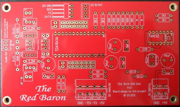
 Photo Details
|
|
|
dvb projekt diyAudio Member Registered: February 2009 Location: Willich, Germany Posts: 1,481  |
The evolution brings the following changes
- Separate I2S-GND route to Digital-GND - Separate Analog Output GND route - Separate GND route for active divider decoupling caps to Analog-GND - Modified active divider decoupling pads for better SMD 1210 caps soldering - Onboard SOT353 footprint for fastest DEM-Synchronizer IC´s - Un-interrupted ground plane - MOSFET Source/Drain failure corrected Still on the module - Direct shunt voltage inputs with shortest onboard traces - I2S In-/Outputs with shortest onboard traces - I2S Attenuator and DEM Synchronizer (by -ecdesigns-) - Onboard Grounded-Gate MOSFET Current Buffer I/V Stage (-ecdesigns- MK7 version) - Separate GND-Trace for DEM-Synchroinizer - Master/Slave connectors for parallel DAC module usage and external I/V Buffer stages e.g. Tube-I-zator & DDNF Stage - no SMD Design |
| Date: Sat February 16, 2013 |
|
| Additional Info | |
| Additional Categories: "Reference" TDA1541A DAC project with I2S-BUS architecture | |
| Direct link: | |