the supply rails will be modulated with the signal.SoundsGreat said:
at 4R0 you might load down your supply.
What exactly you mean ?? ........ transformer for the Nmos200 ! so have to do it based on your recommendation ! I might chose 45VAC (63VDC) ! try to achieve 150W like in your earlier post !! The VA rating will remain 350
The lower the speaker impedance the worse the modulation.
Soundsgreat,even with this transformer
400VA 45-0-45 , a 4 ohm load modulates it and it gets hot
for you , doing a stereo NMOS 200 setup ,get a toroid (runs
cooler)600va like this one-
http://www.antekinc.com/AN-5440.pdf ,
they ship internationally.(IF you can find one there, get it,
shipping is 37$ + 57 for unit =94$)
If you are buying a new transformer any way,
You will get, without modifications, exactly what quasi says
for the 200. 120W- 8R0/200+ -4R0 at +-53VDC w/40000uf.
I built my own boards, already had 4-MJ15003,s so
modified the hell out of the design .mine has 2sc1845
and 4 outputs so I could get 180+ /8 and 250+ /8 with
a bigger PS.
OS.
An externally hosted image should be here but it was not working when we last tested it.
400VA 45-0-45 , a 4 ohm load modulates it and it gets hot
for you , doing a stereo NMOS 200 setup ,get a toroid (runs
cooler)600va like this one-
http://www.antekinc.com/AN-5440.pdf ,
they ship internationally.(IF you can find one there, get it,
shipping is 37$ + 57 for unit =94$)
If you are buying a new transformer any way,
You will get, without modifications, exactly what quasi says
for the 200. 120W- 8R0/200+ -4R0 at +-53VDC w/40000uf.
I built my own boards, already had 4-MJ15003,s so
modified the hell
out of the design .mine has 2sc1845and 4 outputs so I could get 180+ /8 and 250+ /8 with
a bigger PS.
OS.
Fatal Outcomes
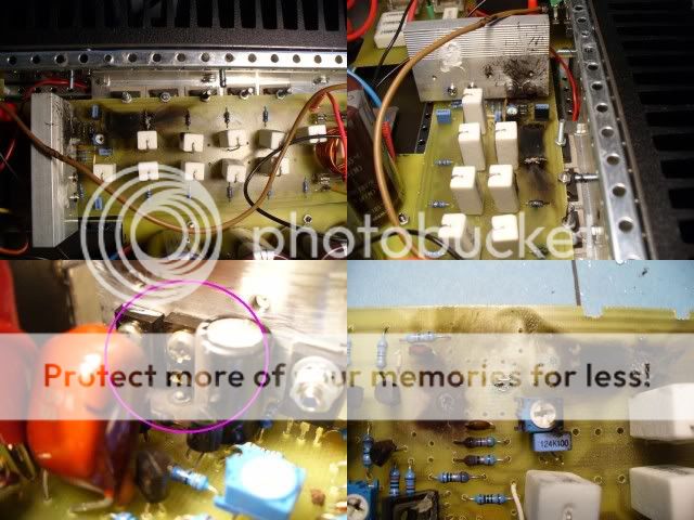
Well ive attached a pic of the mess. I think u may be right, the fet died and took everything else with it. I was using 10A fast blow fuses, the fuse blew of course when the fault happened. I have checked all the FET's, and 6 of them are dead. Im not sure if that sort of thing reduces the lifespan of the 4 remaining fets, and i dont wanna risk it, so im purchasing 10 new ones again.
As you can see on the attached pic, The emitter of T9 has been blown away... the all the gate resistors for the positive rail are dead...
Also, thermal connection was good. The bracket was barely warm (maybe 2-4 deg more than room temp) when it went. Also the other smaller heat sink temperature was warm to touch, but nothing too hot. I did notice that bias currents were rather unstable when i was setting them, could they have fluctuated too much?? any more possible causes?
im going to be alot more cautious with this build, hopefully it has better outcomes...
yeah it was running fine at low volumes for a while (~1hour)... sounding great... this happened when it was turned up...
yeah, the MJE's were insulated. It all worked well for a while.
it could have been what was suggested, one of the FET's failed, making T9 have to drive the load. But that seems like a lot of destruction for just that.... could be wrong...
yeah, not a cheap mistake
yeah, the MJE's were insulated. It all worked well for a while.
it could have been what was suggested, one of the FET's failed, making T9 have to drive the load. But that seems like a lot of destruction for just that.... could be wrong...
yeah, not a cheap mistake
canca87 said:yeah it was running fine at low volumes for a while (~1hour)... sounding great... this happened when it was turned up...
yeah, the MJE's were insulated. It all worked well for a while.
it could have been what was suggested, one of the FET's failed, making T9 have to drive the load. But that seems like a lot of destruction for just that.... could be wrong...
yeah, not a cheap mistake
Hi I built this version with 10FETs but some how Mine was gone and it was as Quasi explained that my output FETs heated up and gone. But in my case the heat sink was very hot. Now I am running the 6FETS Nmos350. That is working really well.
Regards
http://i287.photobucket.com/albums/ll152/Che-babe/Fatal_Outcome640x480.jpg
if looking at this image
the lower left
i can see one eletrolytic cap sitting very close to heatsink + power transistors
If you read data of wet electrolyt caps, you see lifespan at 85 and/or 105 degrees.
This means that temperature will effect the cap's life length.
Now, putting electrolytic capacitor close to something very hot is not to recommend.
Even if cap will not be damaged by +100 degrees or high temperature
it will not be good for the electrolytic liquid inside.
Not in a longer run.
And possibly could shorten the life a great deal.
This is just a sidenote.
It has nothing to do with your current problems with you amplifier.
Not to put electrolytic capacitors close to components/heatsinks that get hot
is one thing good designers of PCB layout should consider
Lineup
Hi, canca87 as far as:
It seems like when T9 turned into a wire, the Vgs of
the IRF's on the positive side were exceeded making them short
which in turn exceeded Vgs of the negative side ...KAboom!
Very logical scenario, well it looks like I put the gate protection
zener's in like I've seen in some nmos amps
(way back in this thread), this mishap is
preventable, fuses would blow first before .
fires and explosions.
PS ..thank you lineup for all IRF datasheets...
OS.
But that seems like a lot of destruction for just that.... could be wrong...
It seems like when T9 turned into a wire, the Vgs of
the IRF's on the positive side were exceeded making them short
which in turn exceeded Vgs of the negative side ...KAboom!
Very logical scenario, well it looks like I put the gate protection
zener's in like I've seen in some nmos amps
(way back in this thread), this mishap is
preventable, fuses would blow first before
.fires and explosions.
PS ..thank you lineup for all IRF datasheets...
OS.
I'll do better than that, I'll show you:
This is Esp project 101 ,different circuit- same principle..
D1/ZD1 limit Vgs to 12V ,keeping gate from being "punctured"
less likely to catch on fire...
I would do D2/ZD2 different ..gate to V- (quasi correct me if you
see this)since this is a different amp.(Quasi-comp.)
I seen someone else earlier in this thread do this on NMOS 200.
hope this helps,
OS
An externally hosted image should be here but it was not working when we last tested it.
This is Esp project 101 ,different circuit- same principle..
D1/ZD1 limit Vgs to 12V ,keeping gate from being "punctured"
less likely to catch on fire...
I would do D2/ZD2 different ..gate to V- (quasi correct me if you
see this)since this is a different amp.(Quasi-comp.)
I seen someone else earlier in this thread do this on NMOS 200.
hope this helps,
OS
well if thats is going to help stop this happening again, defiantly worth a try...
so how would you find the right rating zener? should it be able to handle a current of 10A (so that it doesnt die before the fuses) and what would its breakdown voltage be? also im guessing the diode needs to be able to take 10A as well, otherwise the same problem would happen, the diodes blow before the fuses...
also, that picture u showed us was for complimentary mosfets. you mentioned doing the NMOS from gate to -Vee, that makes sense. but would that damage the fets connected to +Vcc if their gates were connected to -Vee? (if that question even makes sense)
If ZD1 ever turned wouldn't Q7 vaporize?
most likely... fuses would blow...
but Q8-11 might be spared.$$/cheap factor.(lesser of 2 evils
)P.S. canca87 , t9/10 in the NMOS might still fry but you would
save 25$ worth of outputs (whole purpose of gate protection)
lowering risk of fire
(boy, you had a burnt board)I overlooked something, reverse the stringyou mentioned doing the NMOS from gate to -Vee, that makes sense. but would that damage the fets connected to +Vcc if their gates were connected to -Vee? (if that question even makes sense)
ZD2/D2 on the negative FET's since we are not complimentary.
OS.
It usually means that both halves are 5 amps capable.
It should be easy to verify by cheking the size of the transformer, there will be a obvious size difference between a 500VA and a 250VA transformer
Right now I have a 30 lbs UI-core 2000VA transformer on my desk that needs rewinding to provide more useful outputs than a low (okay, it's 300VA or so) power 42VCT and almost all power on a 80V non center-tapped secondary...
ostripper said:I'll do better than that, I'll show you:
An externally hosted image should be here but it was not working when we last tested it.
This is Esp project 101 ,different circuit- same principle..
D1/ZD1 limit Vgs to 12V ,keeping gate from being "punctured"
less likely to catch on fire...
I would do D2/ZD2 different ..gate to V- (quasi correct me if you
see this)since this is a different amp.(Quasi-comp.)
I seen someone else earlier in this thread do this on NMOS 200.
hope this helps,
OS
this is esp property .... its is not a free circuit for everybody to use.....to my opinion it is not nice to do that
Oh give me a break ...HE LEFT out the resistor values so he could
sell boards. I posted the schema for instructional purposes
only. The circuit is one of the most common topologies around
actually George Sziklai had the patent on on this circuit..
(He's dead now)..
IF I wanted to steal someones intellectual property I am well
endowed to do it... (I have the real schematic).
P.S. are you the copyright police or something. ???
sell boards. I posted the schema for instructional purposes
only. The circuit is one of the most common topologies around
actually George Sziklai had the patent on on this circuit..
(He's dead now)..
IF I wanted to steal someones intellectual property I am well
endowed to do it...
(I have the real schematic).P.S. are you the copyright police or something. ???
try asking ESP first. I bet his response will not be to post his schematics.ostripper said:Oh give me a break ...HE LEFT out the resistor values so he could
sell boards. I posted the schema for instructional purposes
only.
IF I wanted to steal someones intellectual property I am well
endowed to do it...
P.S. are you the copyright police or something. ???
His Email to me was that he preferred that we post a link to his site/schematics.
Be respectful!!!!
not really
and i apologize if my comment made you feel uncomfortable but rod is a nice guy and he allready give most of his projects and work for free in his web pages so this at least we should pay some respect to a person that helps diy comunity ....
thats it
ostripper said:Oh give me a break ...HE LEFT out the resistor values so he could
sell boards. I posted the schema for instructional purposes
only.
IF I wanted to steal someones intellectual property I am well
endowed to do it...
P.S. are you the copyright police or something. ???
and i apologize if my comment made you feel uncomfortable but rod is a nice guy and he allready give most of his projects and work for free in his web pages so this at least we should pay some respect to a person that helps diy comunity ....
thats it
- Home
- Amplifiers
- Solid State
- Power amp under development