Hello guys.
I've made this amplifier and after a change of bias resistors on VAS transistors I forgot to connect GND on front end part of the board when powered it on for some seconds. The components on front end have stressed 80 VDC without central point connected.
When I powered it again correctly several faults appeared: DC offset before was 10-20mV, after fault became negative 100-200mV; voltage drop on 15V Zeners only 4.8V like on 5V Zeners, however they are not damaged, I replaced them; voltage drop on 1.5K feedback resistors - 0.475 on positive side, 0.925V on negative side. On the entering points of front end voltage - 40V on both sides.
I measured all front end transistors and haven't found any significant variations in voltage readings.
Could someone help me to find what's wrong with the amplifier?
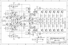
From the schematic I use only 3 output pairs and 40/32 VDC PSUs.
I've made this amplifier and after a change of bias resistors on VAS transistors I forgot to connect GND on front end part of the board when powered it on for some seconds. The components on front end have stressed 80 VDC without central point connected.
When I powered it again correctly several faults appeared: DC offset before was 10-20mV, after fault became negative 100-200mV; voltage drop on 15V Zeners only 4.8V like on 5V Zeners, however they are not damaged, I replaced them; voltage drop on 1.5K feedback resistors - 0.475 on positive side, 0.925V on negative side. On the entering points of front end voltage - 40V on both sides.
I measured all front end transistors and haven't found any significant variations in voltage readings.
Could someone help me to find what's wrong with the amplifier?
From the schematic I use only 3 output pairs and 40/32 VDC PSUs.
Attachments
Last edited:
There is something wrong with that schematic.
How does the input section get power?
What's wrong with this schematic for 3 output pairs? It gets power from separate PSU.
When speaking about BJTs I wouldn't rely on voltage measurements in order to check if they are defective or not. Just unsolder all 8 transistors of both inputs and measure them old fashion way (or measuring Hfe with multimeter).
Do you think the problem in 8 center transistors? I thought it could be a top or bottom pair of transistors
There is something wrong with that schematic.
How does the input section get power?
The drawing might be confusing. Look at the 15V zener. From here it is a current source for the input emitter which is 0.65V.
")
Measure all the resistors and transistors.
Resistors: just check the values roughly. Maybe there will be some surprise.
Transistors: without desoldering simply with the DMM diode tester mode.
NPN: the positive probe to the base and the negative first to the collector and then to the emitter
PNP: probes switched, everything else the same
And the values should be around 4-5-6-700...
Then check all the diodes as well even the zeners.
In a typical case these general measurements are enough to localize the failure.
Hi.
Thank you for your reply.
There won't be a surprises because the amp worked before I mistakenly turned it on without Input GND point. Only bias current on OP devices didn't worked correctly before the fault. Also I changed 33R on drivers MJE15031/30 to 100R to raise the bias current on OP transistors. All resistors measure as they should be.
I already measured all small transistors with desoldering with diode and hFE tests and they all appeared to be fine. Also if on all four 10R emitter resistors of the input transistors I have around 30mV that means all eight input transistors are fine. If I raise a bias current on those emitter resistors (to 30mV approximately), a voltage drop on 1.5K feedback resistors start to differ between them (could be 0.650V on top and 0.910V on bottom resistor). Before the desoldering of small transistors the difference on feedback resistors after the fault was much bigger - 0.465V (positive side)/0.930V (negative side) and when I measured the voltage drop on the negative side feedback resistor my bulb tester was blinking when the voltage drop on feedback resistor reached 1V and again from 0.6V to 1V, some kind of instability appeared after the fault.
I've checked Zeners and the capacitors paralleled to Zeners, 1n4148 diodes, they are all fine, LEDs are glowing. Only on 15V Zeners there is 6,5-7V voltage drop, however should be 15V as before. On 2.2K 2W resistors voltage drop 29.5V approximately.
When I increase a bias current of input transistors more than 30mV (42.5Ohm on POTs, before was 46.5Ohm), the amplifier become unstable and I can't measure the voltage drop on emitter resistors, voltage drop on 15 Zeners now 3.5V, before was 7V
Last edited:
Theres interconnection (kirchoff) between ccs bias current, feedback current and input emitter current. Try to bypass the ccs with a trimmer (10k) you will see that you cannot bias too high without affecting the surounding o.p. If you want a stable reference you can take directly from rail but the mod wont be pretty. Better replace the ccswith a resistor (or trimmer) and bias normally (1ma?). How much current does your ccs output btw?
I think the problem is likely at the IPS (InPut Stage).
With the OPS (OutPut Stage) everything looks good?
You can half the amplifier and check the IPS and the OPS separately.
The VAS (Voltage Amplification Stage) is the end of the IPS at the common
nodes between the 2SA1478/2SC3788 transistors and the 2R2 resistors.
Disconnect the collectors from everything and connect them together.
The other point is the FB (FeedBack) which you should disconnect from output
and connect it to ground. With this arrangement you can test your IPS without
the OPS (not even powered) and check the quiescent voltages and currents.
If all resistors/pots looks fine check those 15V zeners:
unsolder them and give them the same voltage with
the 2k2 resistors and check their voltages.
Likely they will be ok and one (or more) of the IPS transistors shunts them.
Please measure all the voltages on the 10R resistors which are in series
with the input transistors and also measure the V on the 220R resistors.
OPS test: instead of driving it with the 2 VAS output nodes just use two
resistors from the rails and you can check the quiescent circumstances easily.
The actual resistor values should be calculated based on the VAS current.
For example if it's 6mA and IPS rails are +/-40V, the total value should be:
80V / 6mA so 2 pieces of 6k8 should be ok.
But do not forget this Iq (quiescent current) defines the bias voltage
for the OPS so a bigger current means more Iq on the output devices!
The top and bottom pairs are the usual two-transistor constant current source. They bias the input transistors through the 10 ohm resistors.
The current through the collector of the topmost transistor is the bias current of the ccs. Mixed with feedback current it biases the input transistor thru the 10 ohm.
So you can bypass the ccs by pulling out the two transistors and have a trimmer from the 15v zener point to the topmost collector point (or to the 10R). You can also connect the bias trimmer between the 10R and the rail ala PeeCeeBee.
If the trimmer or the bias is taken from the 15v point instead of the rail, 10k trimmer is sufficient. With the original ccs you increase input bias current by lowering the MT100. Measure the bias current. Its more or less the current thru the 10R. With lower rail such as your 40v there is a possibility that with high bias the 15v reference cannot be maintained. I think its a normal behavior. Thats why i asked the bias current. You should know the bias current in the input, vas and output.
- Status
- This old topic is closed. If you want to reopen this topic, contact a moderator using the "Report Post" button.
- Home
- Amplifiers
- Solid State
- CFP Amplifier - Help Please!