CCS = Constant Current Source
It's the typical active load for a voltage amplification stage.
It provides higher gain because it also reacts to the input signal
and adjusts the current on the amplifier transistor such that
ideally it's independent from the input/output voltage.
It's the typical active load for a voltage amplification stage.
It provides higher gain because it also reacts to the input signal
and adjusts the current on the amplifier transistor such that
ideally it's independent from the input/output voltage.
Attachments
Where and how to measure ccs output?How much current does your ccs output btw?
So you can bypass the ccs by pulling out the two transistors and have a trimmer from the 15v zener point to the topmost collector point (or to the 10R). You can also connect the bias trimmer between the 10R and the rail ala PeeCeeBee.
...Thats why i asked the bias current. You should know the bias current in the input, vas and output.
I should connect 10K trimmers (POTs) from 15V zener and 2.2K 2W point to collector point of topmost transistors of ccs? What about other connections of removed pair of ccs transistors?
Bias current of the input transistors (voltage drop on 10R emitter resistors) 29-33mV, on OPS bias current 0.3-0.4mV now on emitters from one side only, other side 0mV; before the fault the maximum I can increase it was 1.1-1.4mV from one side and 0.7-0.9mV from other side, but I played only with the 500R POT, input bias was 25-28mV.
How to measure bias current on the VAS? And what's "rail ala PeeCeeBee"?
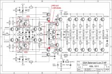
Instead of 2SA1478/2SC3788, MJE15030/31, 2SC5359/2SA1987 on the schematic I'm using 2SA1360/2SC3423, 2SA1930/2SC5171, TTC5200/TTA1943.I think the problem is likely at the IPS (InPut Stage).
With the OPS (OutPut Stage) everything looks good?
You can half the amplifier and check the IPS and the OPS separately.
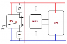
The VAS (Voltage Amplification Stage) is the end of the IPS at the common
nodes between the 2SA1478/2SC3788 transistors and the 2R2 resistors.
Disconnect the collectors from everything and connect them together.
The other point is the FB (FeedBack) which you should disconnect from output
and connect it to ground. With this arrangement you can test your IPS without
the OPS (not even powered) and check the quiescent voltages and currents.
If all resistors/pots looks fine check those 15V zeners:
unsolder them and give them the same voltage with
the 2k2 resistors and check their voltages.
Likely they will be ok and one (or more) of the IPS transistors shunts them.
Please measure all the voltages on the 10R resistors which are in series
with the input transistors and also measure the V on the 220R resistors.
OPS test: instead of driving it with the 2 VAS output nodes just use two
resistors from the rails and you can check the quiescent circumstances easily.
The actual resistor values should be calculated based on the VAS current.
For example if it's 6mA and IPS rails are +/-40V, the total value should be:
80V / 6mA so 2 pieces of 6k8 should be ok.
But do not forget this Iq (quiescent current) defines the bias voltage
for the OPS so a bigger current means more Iq on the output devices!
I also think the problem with the input stage, perhaps some input transistors were partially damaged, as there wasn't such behavior before the fault.
I'll try to put 33R back to 5171\1930 (I tested with 220R and 100R currently).
If I understood you correctly,
I should disconnect the VAS Out points on your diagram and connect them (both collectors) together to each other, feedback point where 1.5K meets I should disconnect from Output and connect both 1.5K to GND.
I replaced 15V Zeners already, no change, previous zeners were fine. Voltage on 220R - 0.506V\0.508V, on 10R from 40V points - 22.9mV\23.7mV drop, on 10R on emitters of input transistors - 23.3\23.5\24.3\22.mV when on 100R POTs was 46.5 Ohm, DC offset was 0-60mV. Al these voltage drops keep changing as well as on 1.5K resistors.
Now with 44.5R on POTs there are 31.3/30.4mv, 32.9/29.5mV on 10R emitter resistors, 0.490-0.510V\0.910-0.960V on 1.5K feedback resistors, bulb tester glows when I touch the first input stage and feedback resistors with test leads, when I keep test lead on feedback resistor - it glows periodically with voltage change on 1.5K.
How to measure VAS current to determine correct resistors to drive the OPS separately?
Last edited:
I've checked the IPS separately without OPS.
V drop on 1.5K was equal 0.660V on both, on 10R emitters 28.2\30.6mV, 34.4\30.5mV, they keep changing. On zeners the same - 5.3V on 15V zeners. I forgot to mention before, LEDs are dimmed, they aren't shine at full power as OPS LEDs when I powered both amp parts. When there is less V drop on 15v zeners LEDs glow more weak if bias increased. Only voltage drop changed on feedback resistors with only IPS powered, before they differ twice.
Can I check the OPS with 4.9K resistors on 2.2R and 56R points powered from the same 32V OPS supply rails? Will I still be able to tune the OPS bias currents with 500R POT?
Last edited:
If it's important, when I measured input transistors after desoldered them, their hFE won't raise as they were new, but were almost steady, if this means something.
Also, after the fault Vbe of input transistors were 0.6V approximately, Vce were: for input pairs - 5.2-6.3mV, for second input pairs which drives the input pairs - 33.9-34.4V, for CCS topmost pair - 4.73-4.96V, for lower CCS pair - 1.267-1.271V, for VAS pair - 3.67-3.78V.
On multiplier transistors Vbe were 0.7V approximately.
How to determine optimal value of base-emitter resistors on the drivers (MJE15030)? LC used different values in his schematics.
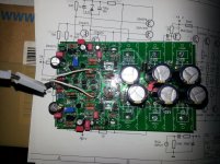
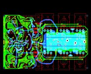
I've added the photos of layout and pcb. I know there are an errors on silkscreen for input transistors and for drivers. I have used only main components on pcb, zeners instead of TL431 by now.
Also, after the fault Vbe of input transistors were 0.6V approximately, Vce were: for input pairs - 5.2-6.3mV, for second input pairs which drives the input pairs - 33.9-34.4V, for CCS topmost pair - 4.73-4.96V, for lower CCS pair - 1.267-1.271V, for VAS pair - 3.67-3.78V.
On multiplier transistors Vbe were 0.7V approximately.
How to determine optimal value of base-emitter resistors on the drivers (MJE15030)? LC used different values in his schematics.
I've added the photos of layout and pcb. I know there are an errors on silkscreen for input transistors and for drivers. I have used only main components on pcb, zeners instead of TL431 by now.
Attachments
Last edited:
Andriy, its hard for me going back and forth to the schema thru a handphone. I kinda talk about the schema from memory. But please follow my logic:
1) Knowing currents will know where things go wrong. You provide V so i must calculate I=V/R.
2) Zener voltage less than 15v (and dimmed led) shows that the zener cannot maintain voltage. Lets calculate what is the "normal voltage". The ccs is taking voltage from the 40v rail thru 4.7v zener thru 2k2/2w and regulated by 15vzener. What is the expected voltage across 2k2? 40V - 4.7V - 15V = 20V. What is the current that will give this voltage drop? I = 20v/2k2 = less than 10mA!
I think that you have more than 10mA or 20v across the 2k2. So what is causing the huge current draw?
CCS is obviously designed to draw current thru that 2k2. Thats why you must measure the output of the ccs. And you have measure 30mv across 10r. This is 30mv/10r = 3mA. With balance input the current output of the CCS is 2X3mA = 6mA, still below the 10mA threshold. So where does the current go? AND WHERE FROM? There are still 2 possibilities and I hope you get the idea to find it by yourself.
You have mentioned VAS Vce=3.7V??? VAS is the cascaded two transistors. The vas output should be several Vbe so you can expect the vas to drop almost all the supply rail. So Vce is huge not below 10 v. If Vce too low then bias string doesnt work, probably a disconnected/broken diode.
If a diode is disconnected, vas output is high and current will go from emitter to base and then to the 2k2 and so on.
Last edited:
Yes you are right, I have 30.6V drop across 2.2K 2W with only IPS powered.
10R on emitters of small VAS transistors have 53mv\41.5mV drop (before were 22.9mV\23.7mV), one side more than double higher with only IPS powered. Vbe of these transistors 0.612V\0.560V, Vce - 3.61V\3.63V. If VAS output of these transistors should be several Vbe, 3.6Vce is 6 times of 0.6Vbe, so they draw too much current? Why? Are they faulty?
Just measured second pair of VAS transistors 1478\3788 on the schematic, 2SA1360\2SC3432 in fact, and found the following: Vbe - 0.718V\0.618V, Vce - 20.4mV\72.8V. Obviously the first transistor doesn't working and could be a cause of such current draw of previous VAS transistors. But how 150V device had been damaged by 80V power supply without central point been connected?
What will differ if I change 2.2K 2W to 1.5K 2W, except more current supply to CCS, as on other similar schematics?
Are 2.2R after the VAS beneficiary? On other schematics they are absent.
Last edited:
You should use a simulator and check there the normal values and compare it with your actual ones.
It's a great tool for tasks just like this.
Try LTSpice for example.
You can use even ideal transistors for beginning to analyize the basics.
I never tried this program. Other members told me that I should have a sim model to simulate this schematic which I don't have and I'm not sure if I'll understand the sim results if I would have the model.
Last edited:
For checking the DC opearating points ideal transitors will be just fine.
It's much more simple then asking us and calculating each section with formulas.
It's very simple to use:
* download
* start
* add the components with F2: just type, npn, pnp, resistor
* set the resistor values using right click
* draw the wires with F3, delete with F5
* once you are ready, run a simulation: Simulate/Edit/DC opt point Ok and then the "Running man" icon on the toolbar
* if there is no error: move the cursor to the nodes and check the voltages/currents
* start with a simple generator + resistor circuit, then add a diode, then a transistor, zener
* if everything looks good, draw your schematic (IPS will be enough for start) and do the same as above.
Good luck!")
It's much more simple then asking us and calculating each section with formulas.
It's very simple to use:
* download
* start
* add the components with F2: just type, npn, pnp, resistor
* set the resistor values using right click
* draw the wires with F3, delete with F5
* once you are ready, run a simulation: Simulate/Edit/DC opt point Ok and then the "Running man" icon on the toolbar
* if there is no error: move the cursor to the nodes and check the voltages/currents
* start with a simple generator + resistor circuit, then add a diode, then a transistor, zener
* if everything looks good, draw your schematic (IPS will be enough for start) and do the same as above.
Good luck!
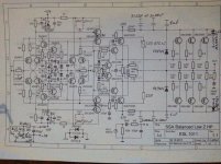
Hello guys.
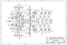
I've made this amplifier and after a change of bias resistors on VAS transistors I forgot to connect GND on front end part of the board when powered it on for some seconds. The components on front end have stressed 80 VDC without central point connected.
When I powered it again correctly several faults appeared: DC offset before was 10-20mV, after fault became negative 100-200mV; voltage drop on 15V Zeners only 4.8V like on 5V Zeners, however they are not damaged, I replaced them; voltage drop on 1.5K feedback resistors - 0.475 on positive side, 0.925V on negative side. On the entering points of front end voltage - 40V on both sides.
I measured all front end transistors and haven't fount any significant variations in voltage readings.
Could someone help me to find what's wrong with the amplifier?
From the schematic I use only 3 output pairs and 40/32 VDC PSUs.
I assume you have two channels - one good one, one problem channel. Why not just start by measuring all the point to point resistances, with the schematic as your guide, and compare the two channels. That might narrow your search.
Sheldon
- Status
- This old topic is closed. If you want to reopen this topic, contact a moderator using the "Report Post" button.
- Home
- Amplifiers
- Solid State
- CFP Amplifier - Help Please!