R11 should be about 1k or 2k, but my rule of thumb is to pass 1/10 the collector current in the base bias chain. At 5mA VAS current that would make the bias transistor chain current 0.5mA, so 2.2k for R11 is not out of line. The base-emitter resistor needs to be around 1/3 of this or 680 ohms in this case (330 ohms for 1k) and this should be made up from a trim pot plus a series limiter - for example 560 ohms plus a 1k pot. The extra resistor (not shown in the original circuit) stops the q-current rocketing into space.
You won't see differences with R8 in or out- it doesn't need to be there. What it would do is to limit the current during turn-on and slow the input tail current source frequency response down. So I'd leave it out.
The collector to emitter voltage of the current mirror should be at least 0.5V to avoid saturating the transistors. THe collector voltage is set by Q6 base voltage which is set by the emitter voltage and voltage drop across R23. R23 can drop say 200mV or more allowing 200mV across the mirror transistors. So that makes R23 about 47 ohms and R3-R4 can be 100 ohms without too much trouble (they will drop 250mV and Vce of the mirror will be around .55V, so R3, R4 could be 47 ohms too. Or if you reduce the input tail current to 2mA they can be 100 ohms.
This is a very useful rule.but my rule of thumb is to pass 1/10 the collector current in the base bias chain.
It gets used in many areas of electronics.
Apply rigorously for a Vbe multiplier.
R11 should be about 1k or 2k, but my rule of thumb is to pass 1/10 the collector current in the base bias chain. At 5mA VAS current that would make the bias transistor chain current 0.5mA, so 2.2k for R11 is not out of line. The base-emitter resistor needs to be around 1/3 of this or 680 ohms in this case (330 ohms for 1k) and this should be made up from a trim pot plus a series limiter - for example 560 ohms plus a 1k pot. The extra resistor (not shown in the original circuit) stops the q-current rocketing into space.
You won't see differences with R8 in or out- it doesn't need to be there. What it would do is to limit the current during turn-on and slow the input tail current source frequency response down. So I'd leave it out.
The collector to emitter voltage of the current mirror should be at least 0.5V to avoid saturating the transistors. THe collector voltage is set by Q6 base voltage which is set by the emitter voltage and voltage drop across R23. R23 can drop say 200mV or more allowing 200mV across the mirror transistors. So that makes R23 about 47 ohms and R3-R4 can be 100 ohms without too much trouble (they will drop 250mV and Vce of the mirror will be around .55V, so R3, R4 could be 47 ohms too. Or if you reduce the input tail current to 2mA they can be 100 ohms.
Very good lesson, thats i need!
Well i'm going for shoping (resistors). Stay tuned....
")

R3-4 are 100R, R23 are 47R, R21-22 i try 100 and 220R too...
R3 280mv across resistor, R4 350mv across resistor, R23 4.5v (yes, volts, not millivolts......) across resistor.
And the piece of cake, 36vDC on output.......
Something goes too wrong here and isnt schematic, and not pcb....
Maybe fake transistors? i buy them from my local electronics store, not internet....
in one channel, Q6 and Q8 are blown, im replease them and the problem remains....
Now nothing is blown up but i have 36vDC to output....
I'm try different values about R3-4-9-23 but with no results....
Whats going wrong here?
Maybe is better to cancel mirror current (Q3-4) and R5-6-7?
Now nothing is blown up but i have 36vDC to output...
36 volts on the output means that your VAS collector is being pulled up because of high base input voltage...i have posted this before, see my post #28, get this right and your output offset dissapears....
on the other side of the scale, if your VAS base voltage is too small, then you are going to have negative offsett at the output....
suggestion:
R9 is a 220 ohm resistor, put a 470 ohm trimpot in series and set your VAS base input voltage so that output offset is zero...
Maybe is better to cancel mirror current (Q3-4) and R5-6-7?
Oh , no ... mirrors are good.
Am working on a similar amp. Built and listened to it 4 years ago.
(supersym BX)
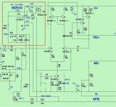
Look at the example (below) ... feel free to use it - it works !
In fact , compare to yours to find the "key" .
...set it up for 45V rails/BCxxx/Mje-BCxxx.
PS - the Q6 / D5 will make for a pure amp that clips nice !!
The red boxed servo is advanced - C8/9 caps are fine , just a little more offset.
EDIT - use the schema as a reference , this design has VERY wide tolerances.
..... integrate with yours !
EDIT 2 - for your EF2 ... 7-10ma VAS is better (R16/17 - 2.2 and 2.7K = 8.5ma @ 45V)
OS
Attachments
Last edited:
If output is +36V DC then either the pull-down/bootstrap resistors are OC, or the bias stabiliser transistor is OC, or the current mirror transistors are OC (especially the first one). After a blow-out it is worth checking all your transistors, and then checking all the connections.
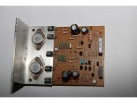
I would use a BD139 for the bias stabiliser and mount this with the drivers and output transistors all on the same heatsink. OK- this may not be so nice if the heatsink is separate due to the additional wiring, but if you put the transistors on an aluminium bracket then they can be wired up to the PCB. See my photo of a very similar circuit I made several years ago.
I would use a BD139 for the bias stabiliser and mount this with the drivers and output transistors all on the same heatsink. OK- this may not be so nice if the heatsink is separate due to the additional wiring, but if you put the transistors on an aluminium bracket then they can be wired up to the PCB. See my photo of a very similar circuit I made several years ago.
Attachments
multisim they havent wrong models, but now im not sure about simulation..... something goes wrong, maybe multisim....
john-ellis what you mean with "OC"?
i have +36vDC on output, transistors are all checked and good for now. burned transistors are repleased with new.....
i'm thinking re-drawing schematic and pcb from zero. to make my self sure.....
john-ellis what you mean with "OC"?
i have +36vDC on output, transistors are all checked and good for now. burned transistors are repleased with new.....
i'm thinking re-drawing schematic and pcb from zero. to make my self sure.....
Hi
I would look at a few basic circuit guides to see how to set currents in transistors.
OC=open circuit BTW.
As a rough guide we normally take the base voltage of a silicon transistor to be 0.6V. So for example the current in the input diff pair current source is set by the voltage between the emitter and - rail and the resistor between those points. Using a red LED sets the base voltage to about 1.6, making the emitter resistor voltage drop 1V. The current will then be 5mA if the resistor is 200 ohms.
In a diff pair the currents should be equal so half should go each way. That makes 2.5mA for each transistor.
On the other hand the VAS current is set in your circuit by the bootstrap resistors which are 3.9k each making a total of 7.8k and at 35V this makes the VAS current 4.5 mA.
I think most VAS currents are too low. To set them you need to calculate the maximum output current needed, then the base current needed for the output transistors, then the base current needed for the drivers. The VAS current should be at least 2x this value, but note that the smaller the max/min ratio the more linear the stage will be.
If the VAS current is 5mA the voltage drop across the emitter resistor is 5mA x R or 235 mV for 47 ohms.
THe voltage you can allow for the emitter resistors in the current mirror should be such that the transistors operate in a normal forward mode (Vce>=Vbe) so I'd suggest that 100mV drop would be desirable, making these resistors 47 ohms also. Then if one side conducts all the current the voltage drop is still only 200mV.
I agree with Andrew T that higher voltage drops make for better mirrors, but 100mV is at least a minimum.
Hi
Just to give you some more clues, I note that your original diagram showed parallel BD911/912 transistors in the output. For 80W into 8 ohms you need 36V which means a peak output current of 4.5A - but in reality more current may be required as speaker impedances aren't constant or 8 ohms. But, the min, gain of a BD911 is 15 at 5A and estimating the min. gain at 2.25A (for each of the pair) it is usefully 20. This means you need a driver current of at least 225mA (worst case). Unfortunately the MJE340/MJE350 are high voltage low current transistors and do not have a good gain at 225mA. They are in fact rated at only 30 at 50mA. Another clue as to their use for high voltage is that there is a high increase in gain with collector voltage, indicating a relatively high collector resistance (which fits in with it being a high voltage transistor).
You can allow 10V as a minimum across the MJE340/350 but this is inefficient. The typical gain for 225 mA is 50 (at 10V) but 25 (at 2V). I would not recommend these as drivers. But just to make the point, if you wanted to use them the base current could be as much as 9mA which is twice what you allowed in your VAS. I would urge you to use BD139/BD140 which can operate to 80V (in fact the original spec. called for 100V BVcbo, but some manufacturers do not adhere to this) and have a gain of min. 65 at 150mA, perhaps worst case being around 50 at 225mA, which needs 4.5mA. Therefore this illustrates my point that VAS currents are usually set too low. You would need IMHO 10mA in the VAS at least, and you could specify higher gain driver transistors e.g. BD139-25 which have a gain of around 250 (typ).
Rgds
John
Last edited:
You're right, I finally calculations fell apart, so the amplifier can not be started.
What I have to do is to gather information and to redesign the amplifier from schematic to printed circuit.
I would like to thank you engaged to fill my head with valuable information that are unable to understand from books.
I will return in a few days with new design and more careful selection of semiconductor.
Hello to all group again!
I'm here with new design and several updates to schematic.
So as you can see, the multimeters are:
XMM-1: R4 drop voltage
XMM-2: R5 drop voltage
XMM-3: Q3 CE voltage
XMM-4: Q4 CE voltage
XMM-5: Q6 AC base voltage (DC are 54vDC)
XMM-6: Q6 bias mA (at idle)
XMM-7: Q8-9 bias mA (at idle)
XMM-8: Q10-11 bias mA (at idle)
XMM-9: Q12-13 bias mA (at idle)
XMM-10: output transistors mV (DC) measured across emitter resistors.
XMM-11: output DC offset.
Changes:
Led are red (1.83vDC drop voltage).
Q1-2-3 are selected 2N5551, bigger VCE and hFE. biased are 5mA. why? bigger trafo.....
R10 are now 200R from 220R,
R13 are 43R to keep drop voltage across R4 to 243mV, why? bigger trafo......
R17-18 are 2.7k for 10.1mA bias to VAS.
The vbe multiplier are now BD139 from BC546 as the original schematic.
R19-20 are connected through the output (is that correct or to put a single resistor emitter to emitter?) and selected to 40R to provide 12mA bias current to drivers.
R23-24, R25-26, R29-30, R31-32 can be pair of 0.47R 2W or single 0.22R 5W.
R21-22-27-28 are 4.7R base resistors to isolate the voltage differents....
R40 are 10R resistor from power ground to signal ground.
And the output zobel network are selected to 10R 2W resistor and 0.047μF cap.....
Some info, i've selected the input network from rod elliott's P3A
C1, R1,R2,R3,C2. i dont know but i see it better from mine.
And gain of amplifier too (R11, R12, C4).
So i think that design will be work.
The trafo are 40-0-40vAC, 700Watt from my old PA Amplifier thats not excist any more.
If i want to keep my original trafo (+/- 39vDC) i can change R17, R18 to 1.8k to provide 10mA to VAS, R19,R20 to 55R to provide 12mA to drivers and R13 to 47R to keep the drop voltage on R4 to 243m
Quiescent current can be adjust from R15 (2k trim pot)
Output DC offset is adjusted from R8 (1k trim pot).
Opinions?
if you use 80V devices that can swing nearly rail to rail, then the absolute maximum rail voltage will be +-40Vdc.
To allow for mains voltage variation and variable sag depending on how many amplifiers are active, you should probably be aiming for +-35Vdc.
To use +-55Vdc and add on variations giving ~ +-61Vdc you would need all the rail to rail devices to be >120Vce0 and preferably ~150Vce0
To allow for mains voltage variation and variable sag depending on how many amplifiers are active, you should probably be aiming for +-35Vdc.
To use +-55Vdc and add on variations giving ~ +-61Vdc you would need all the rail to rail devices to be >120Vce0 and preferably ~150Vce0
Hi
The highest rail voltages I would use with BD139/BD140 is +/- 45 but then I would check that they can withstand 100V. All ST and ON semi devicesI have tested so far can, but as I mentioned earlier, some data sheets give Bvcbo as 80 (should be 100).
Even though BD243/244 might do 100V the second breakdown current is low.
It would be safe to keep to +/- 40V on load with slightly higher voltage at low output.
Alternative drivers (if you want 100W instead) would be MJE15032/MJE15033, or, for higher gain, 2SC4793/2SA1837 and output transistors MJ21193/MJ21194.
But you probably won't have enough gain for low distortion - I would advise using a Darlington VAS for 100W.
But otherwise your new circuit seems to be going in the right direction.
John
Last edited:
Hi
The highest rail voltages I would use with BD139/BD140 is +/- 45 but then I would check that they can withstand 100V. All ST and ON semi devicesI have tested so far can, but as I mentioned earlier, some data sheets give Bvcbo as 80 (should be 100).
Even though BD243/244 might do 100V the second breakdown current is low.
It would be safe to keep to +/- 40V on load with slightly higher voltage at low output.
Alternative drivers (if you want 100W instead) would be MJE15032/MJE15033, or, for higher gain, 2SC4793/2SA1837 and output transistors MJ21193/MJ21194.
But you probably won't have enough gain for low distortion - I would advise using a Darlington VAS for 100W.
But otherwise your new circuit seems to be going in the right direction.
John
Hi, with 39v rails i will be fine... but my thinking is was to make it more powerful, isn't problem...
Maybe my next project is more powerful, quasi complementary, i have 12 MJ15022 in my warehouse and trafo about 40-0-40vAC 700watt (that trafo i'm talking before) and seems good project for sub amplifier.....
I'm going design my new PCB, thanks for help! Stay tuned!
- Status
- This old topic is closed. If you want to reopen this topic, contact a moderator using the "Report Post" button.
- Home
- Amplifiers
- Solid State
- Help for quiescent current adjustment