does this have any effect on stability margins?you may want to bypass R13 with a 1000ufd 6.3volt cap, this increases open loop gains some more...
Similar design.
Simulation result:
Phase Margin = 87 degree
Gain Margin = 16 dB
Slew Rate = 76 V/µS
THD at 162W/8Ohm, 1kHz -> 0.012662%
THD at 162W/8Ohm, 20kHz -> 0.016203%
THD at 324W/4Ohm, 1kHz -> 0.017395%
THD at 324W/4Ohm, 20kHz -> 0.020249%
PSRR at 1kHz -> 108 dB
Simulation result:
Phase Margin = 87 degree
Gain Margin = 16 dB
Slew Rate = 76 V/µS
THD at 162W/8Ohm, 1kHz -> 0.012662%
THD at 162W/8Ohm, 20kHz -> 0.016203%
THD at 324W/4Ohm, 1kHz -> 0.017395%
THD at 324W/4Ohm, 20kHz -> 0.020249%
PSRR at 1kHz -> 108 dB
does this have any effect on stability margins?
i dont think so.... can a capacitor make the same drop voltage of a resistor?
But is good idea to try it... but not now for me...
Similar design.
Simulation result:
Phase Margin = 87 degree
Gain Margin = 16 dB
Slew Rate = 76 V/µS
THD at 162W/8Ohm, 1kHz -> 0.012662%
THD at 162W/8Ohm, 20kHz -> 0.016203%
THD at 324W/4Ohm, 1kHz -> 0.017395%
THD at 324W/4Ohm, 20kHz -> 0.020249%
PSRR at 1kHz -> 108 dB
seems good design, i want tell me where you find the output devices? i found some but are all fake. And to my local store too.... everythink is fake!
If i want play with these power i choose TO3 devices
")
ps. the R17-18 why are different?
ps2. do you have construct it?
thank you!!
I'm waiting hour per hour the new parts of amplifier, like pcb's, resistors, transistors.... Time to see pic's today!
higher open loop makes for lower distortion....
when you get the amp running you can try this tweak,
voltage rating for this cap is higher than the voltage dropped
across the 43 ohm emitter resistor on the VAS,
the reason for the tweak is that, with the addition
of the emitter resistor, VAS transconductance is lower,
and therefore VAS voltage gain is lower also...
with the cap, voltage gain of the VAS is regained...
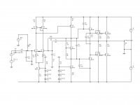
In a comparison I simulated the performance of an implementation of the original but correctly specified resistors, with the "inclusive" feedback version shown below. The main differences are:
low resistances in the feeback arm of the diff pair.
This is not ideal - but the reason is that it maintains the frequency response of the input transistors. You can use D.C. resistances as before instead, if you want a D.C. balance, and parallel an RC network across both the feedback and feedback grounding resistors, which maintains the gain balance except there may be "kinks" if the capacitor and resistor values are not exactly matched. Otherwise, you will need a bias offset resistor on the input side as shown. The offset voltage can be provided by a 1.25V bandgap circuit (for stability) and a potentiometer, or a more comprehensive bias circuit that will compensate for temperature (and hence gain variations as well as Vbe) but that adds a few transistors (and possibly noise).
Two 100pF local oscillation stopper resistors are used on the driver transistors. If the circuit oscillates, these can be increased a little.
The complementary pair bases are joined by one resistor and bypassed with a capacitor which helps to minimise oscillations. This reduces crossover distortion.
The input pair degeneration resistors are reduced to 10 ohms. This increases the gain and reduces the distortion.
A constant current transistor is used instead of a bootstrap. A bootstrap however can be used. VAS current is set at 10mA.
THese mods reduce the overall distortion from 0.12% at 20kHz to 0.025% as simulated.
At 100kHz the differential pair cope well. In both circuits, however, 200kHz causes the VAS to clip. So as long as the source frequency is below 100kHz there should be no transient distortion.
Attachments
Hello to all! Some news, pcb are ready, all are ok to work but the output devices are fake........... i cant find the originals bd911 bd912 or bd243c bd244c.... the only originals i can find are tip41c tip42c..... is this "safe" for my circuit or to buy from ebay with 1 month waiting to get original devices?
Don't expect Ebay to supply genuine product. Some will be genuine, but we have no way of knwing who is the fraudulent seller and who is reliable.
BUYing samples from the manufacturers is a sure way to get genuine product.
National used to do that for the 3886. It was slightly more expensive than buying through UK retailers.
Onsemi do similar. They charge post and packing for batches of 5 devices, you could "sample" 5 pairs of output devices for the cost of the P&P fee.
Last edited:
Nice to read that..... maybe i go to samples for next project....
So, the amp works today. I found originals BD243C for NPN and TIP42C for PNP (Repleasment for BD244C).
Devices are from ST. I found another trafo and my rails are +/-32vDC now. Better and safe i think. And the sound was awesome.....! Tomorrow i will post pics from finished amp and my work.
Thank you all for the useful info's!!!!
- Status
- This old topic is closed. If you want to reopen this topic, contact a moderator using the "Report Post" button.
- Home
- Amplifiers
- Solid State
- Help for quiescent current adjustment