In some ways, the MOSFETs are the opposite of BJTs. In my 1983 paper, I coined the term "transconductance droop" to describe the class-AB crossover shortcoming of MOSFETs. Later, I believe Doug coined the term "gm-doubling" to describe the crossover problem one runs into when over-biasing a BJT output stage.
Not me, gov.
The term has been around for longer than I've been in the business. I object to it, because I have never thought it sensible to describe output stage behaviour in terms of transconductance when what you are really trying to build is a unity-gain voltage amplifier. I disagreed deeply with Ed Cherry on this.
The term I proposed (not entirely seriously) was "gain-deficit-halving" which caught on about as well as you would expect it to.
I agree that this important point should have been emphasised more in the past. It has its own section in the new edition.Back to suggestions for the next edition ..
I'd like to make a plea that the various schematics be checked for missing details that might lead to self destruction on overload. My particular beef is the emitter follower driving the VAS.
(all references to the 4th edition
eg fig 6.16 : TR12's collector current is unlimited on overload so will kill TR4 on HF overload. A simple 'cure' is a resistor in TR12 collector.
Some of the circuits shown are OK. eg fig 5.24 where Q9 protects both Q10 & Q11. I feel this point needs to be stressed ad nauseum as the emitter follower is an essential part of "Blameless".
Hi Bob
I'm sorry, but I cannot get enthusiastic about such a vague acronym. Three letters just aren't enough to convey the information.
I could settle for TOIMC, (output-inclusive) so we can also use TIIMC. (input-inclusive)
Doug,
I am not trying to get you to be enthusiastic about the term TMC. I'm hoping you'll refrain from re-naming what most others have been using for more than 3 years now.
TMC is no more vague than TPC. Two pole compensation. Let's see, how many different architectures can yield two pole compensation? TPC by itself certainly does not imply a variation of Miller compensation, yet we generally understand TPC to mean a variation of Miller compensation wherein the feedback capacitor is split and loaded to ground at the center with a resistor. BUT, one could certainly have two-pole compensation using only lag compensation networks. Anyway, I hope you get my point and don't insist on inventing your own name for TMC and adding confusion.
Out of respect for you, I chose to reinforce the use of the term "gm doubling" in my book, even though one could make a case that it is also vague to the less-experienced. I happen to think it is appropriately descriptive. TLAs (Three Letter Acronyms) are convenient, but often necessarily vague to the inexperienced.
Cheers,
Bob
Out of respect for you, I chose to reinforce the use of the term "gm doubling" in my book, even though one could make a case that it is also vague to the less-experienced. I happen to think it is appropriately descriptive. TLAs (Three Letter Acronyms) are convenient, but often necessarily vague to the inexperienced.
Cheers, Bob
As I said in my post just above, (#261) I did not invent the term "gm doubling" and I do not like it.
Not me, gov.
The term has been around for longer than I've been in the business. I object to it, because I have never thought it sensible to describe output stage behaviour in terms of transconductance when what you are really trying to build is a unity-gain voltage amplifier. I disagreed deeply with Ed Cherry on this.
The term I proposed (not entirely seriously) was "gain-deficit-halving" which caught on about as well as you would expect it to.
Hi Doug,
Golly! I could swear the first time I came across it was from you! I've been in the business since 1970, but of course that dates me to the point where my memory may not be as good as it used to be
") .
.Both views of the output stage are important, but I think it is important to keep in mind that the departure from unity gain in an emitter follower is directly related to transconductance, thus the importance of transconductance. Variation in transconductance of the stage translates to variation in dynamic output resistance of the stage, and that in turn results in gain variation in the stage when it is loaded. Guess I'm with Ed Cherry on that one (I get rather uncomfortable on those rare occasions when I find myself on the opposite side of the fence from that brilliant man).
For someone who has done such a good job of explaining static crossover distortion, I am surprized that you don't seem to rate transconductance more importantly in the output stage.
Cheers,
Bob
No. Variable Vgs, transconductance...not helpful. You know where you are with a BJT.
Hi
I fundamentally agree but if some sort of Vgs 'adjustment' is made by some sort of error correction this problem can be mitigated to the point it is no longer a problem.
Of course there are some other issues with mosfets that have to be overcome as well such as the effects of Cgd.
Some attention should be given to laterals fets , namely
the Hitachi/Renesas , theses are extremely convenient
devices.
Their lower transconductance compared to Toshiba s verticals
or Hexfets is not a problem as shown by National s app note
for their integrated driver , distorsion is not substancialy
higher than the Toshiba while being notably better than
IRFs.
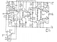
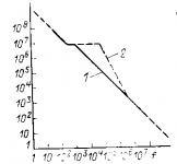
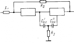
Dear Mr.Self.
pics posted I've found in a rather old book, 1983 to be exact.
It does look like TMC, although the purpose is(was) to design fast settling hybrid op amp...
Being sufficiently ripened I am just curious about the history of analog design.
Image #3 shows the circuit to be placed instead of compensation capacitor Coc1 @ Fig.1.
Boxes on Fig.3 show input stage (left) and VAS (right)
Fig.2 shows open loop gain.
Sincerely,
Alex
Attachments
pure Cherry
.. if I may be so bold as to beg another addition to the next (or future) edition ... though I'm certain Mr. Self will not have time to investigate this to the thoroughness he will want to bring to the subject.
This is to compare TMC and other heresies with pure Cherry as God intended. As an example of what can be achieved using this Holy technique on stone age topologies, I offer post #2321 at
Discrete Opamp Open Design
Further descriptions are at posts #2060 2062 & 2183 on that thread.
This started out as an improved 990 OPA; ie a "Blameless" variant.
Self and practically everyone else have focussed on the VAS having low Zo. This requires the output stage to be a 'perfect' follower.
Alas, the departures from this normally lead to xover and nasty high order harmonics. Self deals thoroughly with these departures and shows that if this approach is taken, it is essential to control Iq to very fine limits.
But what if we current drive the output stage. Then even if the B of the outputs are seriously different, the distortion products (including BJT B reduction with current and yukky Vgs behaviour of MOSFETs) become very low order. Iq is now quite non-critical.
This is why I spurn heretical versions like TMC. These hang evil bits on the critical high Z VAS o/p and even use our valuable feedback to make the output stage Gm more evil.
This is the basis of Cherry compensation. He shows the reduced sensitivity to gm in Feedback, Sensitivity and Stability of Audio Power Amplifiers which I regard as essential reading for guru & pseudo guru alike.
Cherry compensation also maximises the feedback around the most evil stage; the output.
Some people (including Guru Self & even Great Guru Baxandall) have problems getting pure Cherry stable.
I wonder if both these worthies (excuse my use of the 3rd party, Mr. Self) have tried Cherry's own solution to this; an emitter resistor on the VAS (R14 in #2321). If a current mirror is used on the i/p transconductance stage, this does not reduce the open loop gain. My own experience is that Cherry's collector base caps on the driver (evil cos they connect to the VAS output) may not be necessary either.
___________________
Is this guy pontificating through the wrong orifice?
No. I haven't tried this circuit for real. I'm presently a real beach bum and a SPICE newbie. But I have tried pure Cherry on a "Blameless" topology circa 1990. And the SPICE model in #2321 does the things I expect to see in real lifefrom Jurassic experience.
I feel the advantages of pure Cherry are so great as to be worth a lot of effort dealing (with perhaps mythical) instability. To see crossover @ full power 20kHz disappear with less than 10mA Iq, leaving only 2nd & 3rd, was very satisfying.
___________________
I also think when Mr. Self starts investigating a topology that doesn't rely on tightly controlled and small Gm, he will take a less jaundiced view of MOSFETs.
In my case, Cherry compensation opened up the use of evil vertical MOSFETs instead of the Hitachi lateral MOSFETs I favoured in dem days for their nicer 'gm' properties.
Last edited:
There is some more on this useful technique, and more on bootstrapping in general, which (surprise) is not as straightforward as it looks.
That resistor was pure dim-wittedness on my part. The original idea was to protect the circuitry if the CCS failed short-circuit; actually very unlikely. The disadvantage is that the voltage drop across the resistor means that when you are variac-ing up the supply from zero the amplifier will not work until the rails reach some +/-9V. By that time damage may have been done if there is a fault. Without the resistor, you can get a visibly good sinewave with only say +/-3V and the operation is much safer. This is dealt with on p511 of the 5th edition. I hope I have by now removed all those resistors.
There will be a good deal more on the characteristics of the audio signal.
Thanks for clarifying the point about the CCS as emitters load for the input stage.
Will be the Elektor amp with the output stage based on 5532s will have a dedicated chapter ?
six inch long
Your email ended with the words "Oh well". If you have the right tool, you could do a search on these words.
What? Six inches long? That is more appropriate for certain human attributes. For amplifiers however, in particular with MOSFETs in the O/P stage or in case of output inclusive compensation, this is way too long. If your amps can stand this length, they must be very stable.
Shunt is shunt, no matter how large the caps are and no matter how well the supply rails are decoupled to ground. Cherry stated that these caps are crucial for stable performance. So if it is not (a mild) shunt compensation, what else it could be?
Cheers,
E.
Not so far, I'm afraid. I have done a bit of searching but nothing has so far emerged.
Your email ended with the words "Oh well". If you have the right tool, you could do a search on these words.
How long is too long? The Blameless amplifiers are certainly quite happy with 6 inches or so, (probably much more) and I would expect any workable design to be not very different. I don't recall all the details of construction after this length of time but I am sure I would remember something eccentric like extra-long leads to the output devices.
What? Six inches long? That is more appropriate for certain human attributes. For amplifiers however, in particular with MOSFETs in the O/P stage or in case of output inclusive compensation, this is way too long. If your amps can stand this length, they must be very stable.
I assume you are referring to the two 33pF capacitors in the ETI design? That is not shunt compensation- they would have to be very much larger for that. They look very much as if they were added to suppress parasitic oscillation in the output stage; a connection to ground would be better to avoid the possibility of injecting rail noise. This technique is dealt with on p222 of the Fifth edition of Audio Power Amplifier Design.
Shunt is shunt, no matter how large the caps are and no matter how well the supply rails are decoupled to ground. Cherry stated that these caps are crucial for stable performance. So if it is not (a mild) shunt compensation, what else it could be?
Cheers,
E.
squabbling about acronyms
Hi Bob and Douglas,
There is one more reason why TMC isn't that vague. Admittedly, it's true that more than only one TMC configuration is possible. But, since it is the output stage that produces the most distortion, it's obvious that TMC should be applied to this stage, instead of applying it to any other stage, which has far less effect. So it's very unlikely that the acronym TMC might cause confusion.
>for more than 3 years now. Five years, to be precisely. See: http://www.diyaudio.com/forums/soli...terview-negative-feedback-75.html#post1167958
Now that we are already squabbling about acronyms, who the hell has invented 'VAS'? It is a trans-impedance stage and should be called 'TIS'.
Cheers,
E.
Doug,
I am not trying to get you to be enthusiastic about the term TMC. I'm hoping you'll refrain from re-naming what most others have been using for more than 3 years now.
TMC is no more vague than TPC. [...] Anyway, I hope you get my point and don't insist on inventing your own name for TMC and adding confusion.
[...]
Cheers, Bob
Hi Bob and Douglas,
There is one more reason why TMC isn't that vague. Admittedly, it's true that more than only one TMC configuration is possible. But, since it is the output stage that produces the most distortion, it's obvious that TMC should be applied to this stage, instead of applying it to any other stage, which has far less effect. So it's very unlikely that the acronym TMC might cause confusion.
>for more than 3 years now. Five years, to be precisely. See: http://www.diyaudio.com/forums/soli...terview-negative-feedback-75.html#post1167958
Now that we are already squabbling about acronyms, who the hell has invented 'VAS'? It is a trans-impedance stage and should be called 'TIS'.
Cheers,
E.
I am curious about a topic that involves both DS's query and Bob's enthusiasm for output triples and MOSFETs.
In the chapter on OutputS there is a CFP + EF triple shown (p 156 pic. 6.17b of 5th Ed.) and the comment is made that it looks to have "promise".
It looks so to me too, that it combines the best points of a CFP that DS advocates with the triple that Bob likes.
So a follow up on this promise would be of interest.
The CFP stability is of course a concern so more material here would help too.
It occurs that a MOSFET as the second transistor could provide some extra bandwidth that would allow more flexibility to compensate the CFP internal loop. Would the BJT buffer the problematic MOSFET capacitance variation?
In view of Bob's comments above and DS's observation that "it is... wise to consider whether BJTs or FETs are the best devices for the job" do either of you have any comments?
Best wishes
David
Hi David,
Sorry to be so slow in responding to your question. It is a good question.
I always recommend some sort of Triple for any high-quality BJT amplifier. Doubles just don't provide enough current gain under worst-case conditions, especially when high output currents are involved and the beta of the output devices is drooping (and maybe that of the drivers as well). A 50W, 8-ohm amplifier with one output pair delivering 100W into a 4 ohm resistove load must deliver 7A peak from the output device. The MJL21193 will have beta drooped down to as low as 25. With a driver with a beta of 40, the VAS will have to supply 7mA. Things get worse with real-world speaker loads. My rule of thumb is that the VAS should never have to deliver more than 10% of its standing current to the output stage. This would suggest a needed VAS standing current of 70mA to satisfy my rule of thumb. Similarly, with an output double beta of only 25X40=1000, the impedance seen by the VAS when driving 4 ohms is only 4k.
Among Triple output stage candidates, I do not recommend the use of A CFP output pair for the reasons I explained in my book in chapter 5. However, if one must use a CFP output pair, the two safest approaches to achieving a Triple are to precede the CFP with an emitter follower, either conventional or folded. I'm not sure that using a MOSFET in a CFP output stage would help much, but I have not tried it. If the MOSFET is the output transistor of the CFP, then the inevitable gate voltage differences from device to device would translate to a fairly wide range of standing current in the first (BJT) transistor of the CFP. Moreover, the moderately high forward gate voltage needed to turn the MOSFET on to high current values (sometimes 8V), would cause significantly reduced voltage headroom in the output stage.
With an emitter follower output, there are at least three ways that can provide a Triple. The first and most obvious, and probably most used, is the Locanthi T circuit, which is really just three emitter followers in tandem. The second is the Diamond Buffer Triple (DBT) that I described in my book. It just precedes the output emitter follower with a diamond buffer. The third is to precede the output emitter follower with a CFP driver pair (A CFP is OK when used as a driver). The DBT is the most complex because of its need for current sources from the rail, but it has some nice properties.
Cheers,
Bob
Hello Douglas,
Since you took the trouble to ask for opinions, I feel compelled to respond. Here are some of mine in ref to your book. I know you have strong views so please feel free to use these views or lose them as you see fit.
(these are based of volume 4 so may be completely irrelevant to the latest update )
1. why in the preface of volume 4, do you sell the book on its designs that provide " pleasingly reliable and repeatable results with moderate amounts of negative feedback, and insignificant added cost." when you later appear to disparage the "low feedback" school of thought. I'll cite for example the following: from pp 47 onwards
"All of the comments quoted below have appeared many times in the hi-fi literature. All are wrong.
Negative feedback is a bad thing...."
And then:
"A low negative-feedback factor is desirable. Untrue; global NFB makes just about everything better, and the sole effect of too much is HF oscillation, or poor transient behaviour on the brink of instability."
And further :
"The vital point is that if enough NFB is applied, all the harmonics can be reduced to a lower level than without it. The extra harmonics generated, effectively by the distortion of a distortion, are at an extremely low level providing a reasonable NFB factor is used. This is a powerful argument against low feedback factors like 6 dB, which are most likely to increase the weighted THD. For a full understanding of this topic, a careful reading of the Baxandall series is absolutely indispensable."
If you are for large amounts of nfb, appropriately applied, why don't you state as much in the preface instead of referring to moderate fb designs.
2. It may be helpful to avoid sweeping generalizations such as "Two-stage amplifiers are not popular; I can quote only two examples, Randi��3�� and Harris��4��."
The enduring popularity of JLH and Nelson Pass two stage designs seem at odds with this unequivocal statement. You may want to restate your objections to these as "Despite their apparent popularity, two stage designs make for poor amplifiers because ....."
3. Some additional guidelines for the biasing of the input LTP, given that it is your optimal first stage would be very helpful. For example some design examples highlighting the choice between different BJT input pairs and different standing currents and the relationship between these and thd. This would be be a useful addition to the useful stuff you have covered re the choice of the load resistor given a fixed bias current.
4. Ccs design choices and parameters ala Jung.
5. I can only echo the requests by the other correspondents for better coverage on mosfets and CFAs given the popularity of both.
Most humbly,
An ardent reader.
Last edited:
So it's the same but different? What's the point the acronym or name we call something? There is fundamentally different behavior for two amplifiers that are distinguished by what has been an industry accepted nomenclature.
Are you aware that current feedback means the feedback is derived in series with the load (series derived) and applied in parallel with the input signal (shunt applied)?
This gives a closed loop current amplier. The term current feedback does not apply to any other arrangement.
It certainly does not apply to the so-called "current feedback" topology popularised by the IC industry.
Just because the so-called "CFAs" use a single common emitter stage at the most basic level for the input rather than a differential pair does not make them "CFAs".
Read the following definitions carefully please:
http://www.diyaudio.com/forums/soli...current-feedback-amplifier-8.html#post3414948
Dear Mr.Self.
pics posted I've found in a rather old book, 1983 to be exact.
It does look like TMC, although the purpose is(was) to design fast settling hybrid op amp...
Being sufficiently ripened I am just curious about the history of analog design.
Image #3 shows the circuit to be placed instead of compensation capacitor Coc1 @ Fig.1.
Boxes on Fig.3 show input stage (left) and VAS (right)
Fig.2 shows open loop gain.
Sincerely,
Alex
Looks like 2-pole compensation (TPC) to me.
I wonder if both these worthies (excuse my use of the 3rd party, Mr. Self) have tried Cherry's own solution to this; an emitter resistor on the VAS (R14 in #2321).
Yes. It does not work.
If a current mirror is used on the i/p transconductance stage, this does not reduce the open loop gain. My own experience is that Cherry's collector base caps on the driver (evil cos they connect to the VAS output) may not be necessary either.
They are there with intent to control parasitic oscillation in the output stage. From my experience, I would think they are probably very necessary.
No. I haven't tried this circuit for real.
Whereas I have.
Both views of the output stage are important, but I think it is important to keep in mind that the departure from unity gain in an emitter follower is directly related to transconductance, thus the importance of transconductance. Variation in transconductance of the stage translates to variation in dynamic output resistance of the stage, and that in turn results in gain variation in the stage when it is loaded.
Ultimately, almost everything to do with BJT behaviour is related to transconductance, because that is the basic transistor mechanism. But if you are trying to make a voltage amplifier I suggest it is simpler to work mainly in terms of voltage errors. As an example, see the untangling of Large Signal Distortion on p163-4 of the 5th edition of APAD.
- Status
- This old topic is closed. If you want to reopen this topic, contact a moderator using the "Report Post" button.
- Home
- Amplifiers
- Solid State
- Audio Power Amplifier Design book- Douglas Self wants your opinions