Thanks Struth.Hi Guys
Convention is not necessarily the best way. Leach had output stages oscillate to death with the zobel on the amp side of the coil. If you are tired of Leach, look at Bryston: they place the zobel after the choke, too. Chris Russell and Stuart Taylor are both very smart and tuned-in designers, as is Marshall Leach.
I think even Archie Leach would agree.
The trimpot for DC offset definitely will be problematic in its present position. The concern about performance is real. A less crucial facet is the fact both signal and DC currents are effected by the pot's rotation, so definitely adjust it WITHOUT a speaker in place - unless you like earthquake noises.
Considering the effort so far to create a power buffer with stupendous performance - wide bandwidth, super-low THD - it seems like a major fumble to retain the input offset trimpot. FdW and I seem in agreement on this, but Sakis will only consider Lineup's input for the PCB. His position is understandable considering his effort to design the card, but he has already acknowledged that this is only a beginning: more board designs will be necessary.
Have fun
Kevin O'Connor
I think sakis should really listen to a few more fellows.
That can think of such I havent yet considered.
The whole idea with DIYaudio is to learn from eachother.
Here I post the current directives I have posted in EMAIL on his request.
Feel absolutely free to come forward to help us.
I feel we need a lot of assistance
")
Here you are:
Attachments
I see what you mean. This Buffer became more complex than I like.It works, but can you give a justification for this level of complexity, U5 and U9 could easily make up input stage and vas in a conventional design.
But this is not unusual.
There are so complex preamplifiers for many dollars, when all that is really needed is one single OPamp.
The hunt for perfection costs a lot of complexity.
I can give schematics over amplifiers that are horrendous. Not at all on the level with Doug Self's Blameless.
The input impedance is a around 23 kOhm.To successfully drive this baby, you will need the brute force of a diamond input stage, however you could lower I1 and I2 by a factor of four and other options may open up
An easy load for most preamplifiers or OPamps.
Hi Guys
Complexity is in the ear of the beholder. If one wants a conventional design one should visit a different thread. The design here is actually NEW and INNOVATIVE! If that scares some people, they should hide behind Lin.
My PCB layout for my version of the buffer has all four elements of the diamond feedback buffer in contact. It is a simple matter to set the flats of the 2SA/2SC inputs back-to-back so they can be bolted together. The TO-92s are arranged outside of these with their flats against the TO-220Fs. A rubber band or heat-shrink tube can be used to hold everything in contact. Because of how the pinouts work out, the emitter Rs for the TO-92s must be mounted first, lying between the TO-92 and related TO-220F. No traces have to cross, so a single-sided arrangement can be used for this portion.
My PCB is 4.5x3", with two pairs of outputs, local filter caps and decoupling for the front-end. The addition of current sources for the front-end to make it exactly like the latest Lineup buffer would not make the board much larger if at all.
Have fun
Kevin O'Connor
Last edited:
Struth.
Can you make a drawing of a Tube frontend for this buffer.
Use 6DJ8 in a single tube fashion.
You know the input impedance of the buffer is 22-23 kOhm.
The voltage gain should be like Gv=20 or less.
If you can not do it, I will do this myself.
I have in my SPICE a good model for 6DJ8.
It was actually made by M. Leach, the professor in electronics.
Here are the figures
for Class A version.
Rails are +/- 25 Volt and quiescense current is 1.5 Ampere.
The clipping starts at 22 Vpeak. At 23 Vp it is heavy clipping.
The 20 kHz numbers are really good.
As can be seen from my analyse:
for Class A version.
Rails are +/- 25 Volt and quiescense current is 1.5 Ampere.
The clipping starts at 22 Vpeak. At 23 Vp it is heavy clipping.
The 20 kHz numbers are really good.
As can be seen from my analyse:
Power Supply +/-25 Volt, 8 Ohm load TripleEF_5a Class A
THD 1kHz
04 Vp, 01 Watt THD 0.00006%
08 Vp, 04 Watt THD 0.00004%
12 Vp, 09 Watt THD 0.00007%
16 Vp, 16 Watt THD 0.00007%
20 Vp, 25 Watt THD 0.00010%
---
22 Vp, 30 Watt THD 0.16210%
23 Vp, 33 Watt THD 1.29898%
THD 20kHz
04 Vp, 01 Watt THD 0.00040%
08 Vp, 04 Watt THD 0.00080%
12 Vp, 09 Watt THD 0.00122%
16 Vp, 16 Watt THD 0.00166%
20 Vp, 25 Watt THD 0.00213%
It may work this way.OK ....first attempt for pcb is done
here is some detailed pictures and also large files can be downloaded from my server .
There is also detailed explanation and also someone should double check for errors
Users that also have S-Print layout 4 may also down load a complete file from my server
board size is 135X80
kind regards
sakis
An externally hosted image should be here but it was not working when we last tested it.
An externally hosted image should be here but it was not working when we last tested it.
An externally hosted image should be here but it was not working when we last tested it.
An externally hosted image should be here but it was not working when we last tested it.
But for latest instruction see my schematic I send to you.
Great work Sakis.
You are really clever making PCB
DC Offset etc
Hi, if this was built as a bridged Amp, from what i've read in the past anyway, it "could" solve the DC Offset issues. Also it "might" take care of turn-on/off thumps too.
Not only that, but the output power would obviously increase, assuming the same voltage rails. Alternatively, you could use lower voltage rails & still achieve Very lower distortion for the equivalent power output compared to a single Amp !
Regards
Hi Guys
Zero D, I believe you are thinking of "balanced" amps. With the DC and AC conditions of both pathways connected, there is symmetry of behaviour but no actual guarantee of perfect DC balance despite the moniker. It is really a similar condition for bridged amps, as well.
The DC offset of one amplifier is not going to be matched by another unless a DC servo is there to set them equal In a balanced circuit, a current source with common-mode feedback can achieve this, while also assuring improved AC balance. With conventional bridged amplifiers, the DC offset correction within each amp is the assurance of little or no DC through the load.
"Balanced" PAs are all the fashion now, along with balanced interconnections. For the very high power "super" amps with "super" price tags, balanced operation is the only economical way to achieve high power with common devices. It is really just pre-bridged amplifiers with different packaging.
Single-ended drive of the speaker at least limits the DC "problem" to one circuit.
Lineup, the class-A performance numbers are awesome! People should pay attention to the low-level performance as that is where most actually listen. The high power numbers are equally as impressive and outperform most production amps and even some of the "super" amps.
Saki, is there a way to post a smaller thumb nail that can be clicked on when people want a larger image? I don't know how to do that myself as I can only make PDFs anyway. It would make loading and scrolling through the pages of the thread quicker.
Have fun
Kevin O'Connor
I havent heard from Sakis.
He should be doing the PCB.
But I guess he is busy.
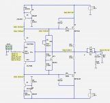
Meanwhile I post a simplified version.
This has Complementary JFET input
and the output is MOSFET IRFP240/9240.
The distortion is a bit higher than for Normal with Triple EF output.
But this circuit is still showing not too bad numbers.
For most applications this will do very well.
.... and it is so simple!
He should be doing the PCB.
But I guess he is busy.
Meanwhile I post a simplified version.
This has Complementary JFET input
and the output is MOSFET IRFP240/9240.
The distortion is a bit higher than for Normal with Triple EF output.
But this circuit is still showing not too bad numbers.
For most applications this will do very well.
.... and it is so simple!
Attachments
Hi Guys
The biggest problem with complimentary jfet circuits is acquiring jfets and matching them.
John Curl famously uses such input stages - complimentary jfet diff amps - in has amps since the 1970s. When he bagen, the range of jfet types was expanding. In recent times, that range has diminished to a great extent. His designs for Parasound are essentially what he has been building for decades, but with a DC servo added, more degeneration here and there to accommodate unselected parts, and other accommodations for production. His own company builds the versions of these circuits with critically selected components and he can only produce a few amps a year at mega-prices. The sim models for jfets will be ideal, reflecting a need for selection and matching for best performance - possibly even for reliable functioning.
Both Curl and Pass bemoan the hunting and hoarding required to be able to sort through and find matched sets of comp jfets. These are very useful devices but industry has generally abandoned the need for p-channels.
If there was a "p-type" tube, you could make the tube version front-end.... Likely be less accurate than the jfet one.
Have fun
Kevin O'Connor
Hi Guys
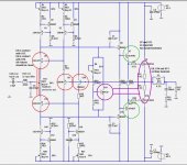
Here is a partial layout, just of the diamond feedback buffer area, to show how two TO220s and two TO-92s can be held in thermal contact. Hopefully the PDF allows colour. In the layout, RED is top copper and BLU is bottom copper as is standard. I set the Q1-4 designations out to the side to make it easier to see them in case the PDF is all-black.
Between the TO-220s there is a top trace that covers a bottom trace over part of their travel. In Eagle (PCB layout software), you can turn off layers to see things more clearly.
The schemo shows R1 and R2 intact, instead of the trimpot. Also, there are base stops for Q3 and Q4.
V+ and V- are the supplies.
CS+2 is the current source that supplies the base of Q1.
CS-2 is the current source that supplies the base of Q2
Drive-pos is the signal drive to the upper EF half
Drive-neg is the signal drive to the lower EF half
Input and output are as they sound.
Have fun
Kevin O'Connor
Attachments
It has not happend much.ok ppl
been away with 39+fever and a terrible stomach can somebody please update me ?
Kind regards
sakis
Good you are well again.
But you should study the suggestion from Struth.
In his last post: http://www.diyaudio.com/forums/soli...ower-follower-output-stage-4.html#post3247993
If you have questions regarding PCB, just send me an email.
I will answer.
- Status
- This old topic is closed. If you want to reopen this topic, contact a moderator using the "Report Post" button.
- Home
- Amplifiers
- Solid State
- New Lineup IDEA - Power Follower/Output stage