With the schottky diodes,MiiB, the simulation file I attached contains the "schottkey mod". It may also have practical value as far as maintaining the distortion profile at high powers, without adding extra active components
how much will the headroom drop?
Max power output into 8 Ohm?
Lineup,
At this current, the load will take up to 1A with the other device just on. Steadily, after this current is exceeded, the inactive output will turn off, making this deep Class AB.
As it stands, around 1A is the limit in Class A, and this corresponds to about 8Vp across an 8R load, which represents 16 exp 2/64 = 4W.
However, that 'First Watt' is the most critical, it should sound wonderful!
BTW, Schottkys should take off no more than 2Vpp off the clip.
Cheers,
Hugh
Last edited:
Mikelm:
1: no DC signal-to-bias gain because the lowered VAS resistor (450R G-S) increases VAS load proportionally to Jfet bias current. Or is this only true for BJTs?
1: better HF linearity because the capacitive currents of the VAS would be smaller WRT Jfet bias.
2: A MOSFET CCS adds plenty of extra shunt capacitance to the feedback node; a proportional phase-lead cap may be needed to correct for this. And even then the shunt cap will change with input voltage. I suggest to try a bootstrap here?
Stability things to try:
1: 1nF from G-D of Jfet.
2: 1nF G-D of VAS (already tried, didn't work).
3: 100pF-1nF from the VAS drain to ground. (I just realized all capacitance nodes from the VAS have been resistively terminated, so the next step is apparently to add a ground-shorting cap with no resistance.)
- keantoken
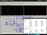
The first image is the THD and FFT from a version with the bootstrap Jfet CCS. The second image is with the bootstrap removed and offset re-corrected.
Instead of odd harmonics being dominant, it's even ones! That's not something you see every day...
- keantoken
Instead of odd harmonics being dominant, it's even ones! That's not something you see every day...
- keantoken
Attachments
Mikelm:
1: no DC signal-to-bias gain because the lowered VAS resistor (450R G-S) increases VAS load proportionally to Jfet bias current. Or is this only true for BJTs?
Not quite sure what you mean here - but I think I agree. Basically, the current in the i/p stage is almost entirely modulated only by small voltage variations across the load / drain resistor - that's it ! I measured this in spice with a mosfet VAS.
2: better HF linearity because the capacitive currents of the VAS would be smaller WRT Jfet bias.
Yes, but these are so small compared to the variation discussed in point 1 I think we can ingore unless we replace the resistor with CCS but even then they are still extremely small. The huge variation compared to all this is a approximate 5% change in voltage across the Jfet with a 1 Volt i/p signal which a the Hawksford cascode will cure. Only after this was implemented would I give a thought to these other very small variations.
3: A MOSFET CCS adds plenty of extra shunt capacitance to the feedback node; a proportional phase-lead cap may be needed to correct for this. And even then the shunt cap will change with input voltage. I suggest to try a bootstrap here?
Thanks for this input I will check to see what impact the FET CCS has on stability. I chose MOSFETs because a want to match i/p stage current variation from MOSFET VAS device with equal and opposite variation from this CCS but actually only the bottom device needs to be a MOSFET. I think Hugh is convinced it won't work but I'm gonna give it a try
")
1: 1nF from G-D of Jfet.
2: 1nF G-D of VAS (already tried, didn't work).
3: 100pF-1nF from the VAS drain to ground. (I just realized all capacitance nodes from the VAS have been resistively terminated, so the next step is apparently to add a ground-shorting cap with no resistance.)
Thx for your input - I'll check 1 & 3 out
mike
Last edited:
More info:
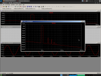
1: Even order harmonics remain dominant regardless of power.
2: Odd order harmonics increase with frequency. (it is likely that even order ones do too as in a monotonic relationship, but this increase is swamped by the already large numbers of even harmonics)
3: High order harmonics also increase with frequency. (#3 and #2 are normal for any amp)
I think that the monotonic profile which rises with frequency, and combines with the even harmonic profile, is the distortion of the VAS, which is capacitively loaded by the MOSFETs and therefore shows increasing distortion with frequency.
- keantoken
So interesting, even this very simple amp under careful analyses is so complex.
If we really want a simple amp then I think we have to forget some of this detailed analyses.
However, if we really want to strive for the best from this simple concept amp there are so many avenues to explore but I think I will have a simple version as a reference to make sure I don't loose more than I gain with these refinements.
I haven't tried "tuning" the bootstrap yet. To an extent I don't think tuning could be done with discrete components because the match here is too good - the experimenter would have to manually tweak using a trimmer.
Mikel, shunt capacitance from the feedback node can be used to decrease HF phase shift (and increase BW) at the expense of OLG. I don't know if the effect on OLG is sonically "good" or "bad" (but I suspect it is good, like a canceling effect on VAS miller currents). If this effect is desired, a series resistor could be added to the capacitor (or MOSFET in your case) which would snub parasitics and increase stability.
- keantoken
reminds me yet again of JLH's VR for a tunable R+C in the inner feedback loopMikel, shunt capacitance from the feedback node can be used to decrease HF phase shift (and increase BW) at the expense of OLG. I don't know if the effect on OLG is sonically "good" or "bad" (but I suspect it is good, like a canceling effect on VAS miller currents). If this effect is desired, a series resistor could be added to the capacitor (or MOSFET in your case) which would snub parasitics and increase stability.
I think this kind of complexity is benign, as opposed to complexity where only THD numbers are improved on at the expense of all other attributes which seem to play a role in the sound of an amplifier.
A THD-centric designer looking at such a circuit may see it as a simple, even "dumb" circuit - even if the design was very difficult for the creator.
So think the circuit is still simple enough - although many difficult options still exist as far as improving it's "sound".
- keantoken
A THD-centric designer looking at such a circuit may see it as a simple, even "dumb" circuit - even if the design was very difficult for the creator.
So think the circuit is still simple enough - although many difficult options still exist as far as improving it's "sound".
- keantoken
I made a simulation tweaking the bootstrap. I stepped the series bootstrap resistor with these values: 56k, 68k, 76k, 86k, 91k.
I was surprised how little it matters! The AC function of the bootstrap here only serves to augment the feedback network, so it makes sense that changing it won't affect the distortion profile.
- keantoken
I was surprised how little it matters! The AC function of the bootstrap here only serves to augment the feedback network, so it makes sense that changing it won't affect the distortion profile.
- keantoken
Keantoken,
Unfortunately my zvp board currently has a bc560 bjt in it, which is plagued with the same problem! I am beginning to think that running under 15ma in the vas might cause unequal charging/discharging of the fet gates and hence oscillation. I know rod Elliot had this problem.
My designs with the bd140 and 9610 were stable, and it is possibly because they were running over 15ma, not because they are slower! Who knows?
My layout is appalling and it wouldn't surprise me in the least if it were to blame. That said, I have managed to tame the other types I have tried with similar layouts. I hope to build a new one tomorrow night, if time permits.
I'm still not even convinced it is worth pursuing this considering it seems stable with a load attached.
Milkelm,
Your proposed circuit looks promising. How long til we get a full review? I hope it lives up to my hype
I began mounting components yesterday, some more things arrived in this mornings post so I'm progressing OK but 3310's are not here yet.
sorry to hear you are still having problems there - your appalling layout does sound like a possible culprit. I hope the time I spent making my boards proves worthwhile coz I could have breadboarded it in about 1/10th of the time.
good luck
mike
In spice the MOSFET CCS to the neg rail does not affect stability at all - replacing with a resistor to the neg rail gives the exact same ringing signature with 100nF at the o/p.
but there is a trade off with choosing FB impedance. Higher impedance FB gives greater stability but raises the noise floor and vice versa.
but there is a trade off with choosing FB impedance. Higher impedance FB gives greater stability but raises the noise floor and vice versa.
Last edited:
Mikelm, if you look at the output impedance you will see that most amps want to behave like an inductor, as seen by the load. This means that with a large enough capacitive load, every amplifier would ring. So ringing is sometimes only an indication of a healthy amplifier. An amp that rings for a long time may just have very low output resistance. A better way to check stability I think is to feed the signal generator into your amp's output through a film cap and sweep the frequency, watching for peaks and dips and distortion.
I like to think that with enough skill, a designer can choose all breakneck options and still have a perfectly stable amp... That is what I aspire to anyways.
- keantoken
I like to think that with enough skill, a designer can choose all breakneck options and still have a perfectly stable amp... That is what I aspire to anyways.
- keantoken
- Status
- This old topic is closed. If you want to reopen this topic, contact a moderator using the "Report Post" button.
- Home
- Amplifiers
- Solid State
- JFET input, MOSFET VAS, LATERAL output = Perfect!!