Hi all,
It has been a good night.
Thank you for your help with the simulation issues.
I now have the simulated oscillation sorted. I have managed to get my simulation oscillating exactly as it does in real life, that is, on the negative half cycle of square waves only. I have found that one way of completely eliminating the problem, in simulation at least, is to add 100pf in parallel with the series feedback resistor. Much less than this and it does not help as much, and much more than this causes its own problems. I think a capacitor here may be crucial to getting the design stable with the zvp3310a. However it is going to require careful trial and error to get right.
I tried a few values in the actual circuit and it definitely helped but the problem persists. I will fiddle a bit more with this tomorrow hopefully.
Another thing I am thinking is that it may be caused by the n channel output fet turning off. However I have tried asymmetrical gate resistors as well as adding capacitance to the n channel fet to no avail.
Anyway, I think the parallel feedback cap shows promise.
Will try more tomorrow and post results.
Last edited:
One thing we might not have thought of is to put a small cap across the gate-source of the VAS. I would try 1nF and 100pF and keep going if either of those values work.
Also, since the ZVP3310A has about 1/50 of the capacitance of the other FETs you tested, you may need a gate stopper 50 times larger.
- keantoken
Also, since the ZVP3310A has about 1/50 of the capacitance of the other FETs you tested, you may need a gate stopper 50 times larger.
- keantoken
Greg & all,
I took a look at the zvp3310a in my DC version and tried to engineer it for maximum stability with least compensation so after checking I added all the features that make the amp fast & stable.
For me there where some compromises - higher value FB resistors are good for stability but bad for DC drift and I am still hoping to manage without a servo.
Also higher value FB resistors - in my design - reduce 1st stage current and I found that higher current helped with stability so I had to add a CC Sink to a filtered neg sub-rail.
High current in the VAS also helps so I went with 2 x 3310 - sorry Greg I can feel you cringing but I think it will be OK - I will build my prototyping board so both options are available.
I decided to allow some ringing with 100nF with no i/p filter but could but could not do away with compensation completely as Nelson has in the F5 - which for me is a work of elegant genius - but I managed to reduce lead compensation to a minimum and with do away with lag compensation.
With a modest i/p filter 100n hardly changes the square wave.
I hope as before that spice & reality are not too far apart.
It has been difficult to choose which version to build but as my 3310's have not yet arrived ( thx 4 the offer ) I will go with the 9610s.
mike
Attachments
Last edited:
One thing we might not have thought of is to put a small cap across the gate-source of the VAS. I would try 1nF and 100pF and keep going if either of those values work.
Also, since the ZVP3310A has about 1/50 of the capacitance of the other FETs you tested, you may need a gate stopper 50 times larger.
- keantoken
Keantoken,
I have tried up to 330pf in this position with no luck! Crazy huh?
Sounds good mikelm, the 9610 has its appeal and extra current it allows may help reduce instability caused by charging the gates at different rates. I know rod elliot has had issues with this.
All of my versions with low stability have had lower vas current so it is possible it is this, and not the actual device that has caused the problems.
I really look forward to your results.
All of my versions with low stability have had lower vas current so it is possible it is this, and not the actual device that has caused the problems.
I really look forward to your results.
Mike.. i believe your CCS'ed version is a huge step up...and with a good size front end cap.. the turn-on thumb is also greatly reduced....
seems like with mosfets that the input capacitance is largely connected to the current capability...we'ed like high current but also low capacitance..which works in opposite directions as the lager die naturally has larger capacitance....It just might might be worth looking into some of the RF devices Vladimir is exploring in his single ended designs...
seems like with mosfets that the input capacitance is largely connected to the current capability...we'ed like high current but also low capacitance..which works in opposite directions as the lager die naturally has larger capacitance....It just might might be worth looking into some of the RF devices Vladimir is exploring in his single ended designs...
Mike.. i believe your CCS'ed version is a huge step up...
Hi,
Yes, I remember you were advocating a CCS earlier in the thread but I still am not sure why. Can you explain why you prefer this.
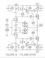
Mr Pass seems OK to drive i/p Jfets straight into the FB network only ( see attached F5 diagram ) so I wonder what your reasoning is.
For me it was simply to combine higher i/p stage current, with higher impedance feedback on this particular design, but apart from this I see no objection to it.
Attachments
When you omit the CCS current through the Jfet varies with the signals applied...so when pushing the amplifier work conditions change....this can be minimized with a CCS.. and that can lead to better DC offset control....
One should also not neglect Wahab's dual BJT VAS.. Though not explored...i have an idea that it would maintain the distortion profile better when the amplifier is pushed...
I'am now contemplating at totally different use for this circuit concept.......More to come in a different thread...
One should also not neglect Wahab's dual BJT VAS.. Though not explored...i have an idea that it would maintain the distortion profile better when the amplifier is pushed...
I'am now contemplating at totally different use for this circuit concept.......More to come in a different thread...
Last edited:
MiiB,
mmm - but the only way to truly control the current through the i/p jfet is to have a mosfet VAS and a CCS as the i/p Jfet drain resistor - this way everything is controlled except HF modulation via the VAS mosfet capacitance or miller cap.
Otherwise with the CCS below the Jfet, the FB network in parallel to the CCS is still modulating the current through the Jfet.
mike
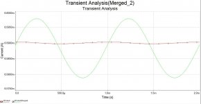
See below currents:
1) with CCS below Jfet from my most recent dual 3310 cct ( green )
and . . .
2) with CCS added as drain resistor ( red )
0.5 Volt i/p @ 1Khz
So, if controlling current is important to you then the i/p Jfet drain CCS is the way to go - however this is not conducive to my goal for this recent project of enhancing stabilty.
( p.s. even more interesting is the phase shift between the current plots )
Attachments
Last edited:
mikelm
You can, should run one transientanalys with output from 2 nodes
(instead of runing two and do merge.)
This way ou get correct timing, for sure.
but I changed the circuit between tests - the node remained the same - so this was the only way in this instance
Correction
The above statement is incorrect
I should have said that the current in the Jfet is entirely dependant upon the slight changes in voltage across the Jfet drain resistor + a tiny amount AC leakage through the FET VAS device.
With a CCS in place as drain load only this AC leakage current remains which is the difference shown in the graph.
Adding a CCS below the Jfet makes absolutely no difference to the current changes through the Jfet but it may favourably increase the ratio between the total current and the variations
Otherwise with the CCS below the Jfet, the FB network in parallel to the CCS is still modulating the current through the Jfet.mike
The above statement is incorrect
I should have said that the current in the Jfet is entirely dependant upon the slight changes in voltage across the Jfet drain resistor + a tiny amount AC leakage through the FET VAS device.
With a CCS in place as drain load only this AC leakage current remains which is the difference shown in the graph.
Adding a CCS below the Jfet makes absolutely no difference to the current changes through the Jfet but it may favourably increase the ratio between the total current and the variations
Last edited:
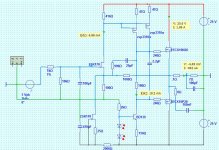
Subject to any further revelations from Greg and the fact that works in real life and sounds as good as Greg says etc, this is the final circuit that I will aim for.
This includes measures for natural cancellation of DC offset based on the same technique that TimA used and Hugh's explanation of the chief mechanism for drift in this design - thx")
I'm still awaiting some bits so for now I'll build with 9610's and a few other differences.
Now time for some sleep
This includes measures for natural cancellation of DC offset based on the same technique that TimA used and Hugh's explanation of the chief mechanism for drift in this design - thx
I'm still awaiting some bits so for now I'll build with 9610's and a few other differences.
Now time for some sleep
Attachments
- Status
- This old topic is closed. If you want to reopen this topic, contact a moderator using the "Report Post" button.
- Home
- Amplifiers
- Solid State
- JFET input, MOSFET VAS, LATERAL output = Perfect!!