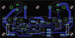
My own take on a layout for Rod Elliots P3A amplifier.
60-80W Power Amplifier
With heatsinks for the drivers transistors, 470uF supply caps on each rail, close to the output transistors. Used MJ15003/MJ15004 NPN/PNP TO-3 transistors for output.
Board is made somewhat long at 160 mm but only 80 mm wide. The extra length is for more spacing between output transistors which should lead to better utilization of the heatsink.
Board is singlesided for easy prototyping and because I can. 🙂
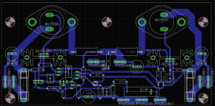
Attachments
Is pin26240 supposed to be the speaker ground? if so, it seems to be floating... 😉
Speaker ground will be at the star ground.
I have +V pin, -V pin, input pin, 2 x input gnd pin of which one should go to the star gnd point, output pin, Zobel gnd pin.
But I might be seperating +V and -V gnd from signal gnd so I get separate supply gnd.
Last edited:
Why? That seems to go against what everyone else here usually advocates. 😕Join all spare copper to ground.
Last edited:
Forgot to mention that the input cap, which is a 4.7 uF electrolyte in the original ESP schematic, has been changed to a 4.7uF film cap instead. Going to use a Evox Rifa MMK 4.7 uF, 63V cap. But theres room for other options as well. 🙂
Last edited:
Hi there neutrality a good pcb layout apart from the proximity of the input cap and the output node should be as far apart as possible.Hope you dont mind me pointing this out. Btw i have made my own pcbs for this design
Hi there neutrality a good pcb layout apart from the proximity of the input cap and the output node should be as far apart as possible.Hope you dont mind me pointing this out. Btw i have made my own pcbs for this design
Dont mind that at all, and a good observation.🙂
Funny, I know they should be apart but somehow didnt think about it when doing the layout.
Thats something Ill look at later today, as well as the separation of input gnd from the other grounds.
I would make Q9 (bias) a TO126 and move its location to mount onto Q5's (driver) heatsink to thermally track, as obligatory for a cfp O/P stage.
Brian.
Brian.
Could one use a bd139 for that as well or should it be something else?
Another thing, Rod Elliot just uses a BC546 for that, with no heatsinking or thermal tracking and it apparently works just fine.
So his design is flawed or?? 😕
Another thing, Rod Elliot just uses a BC546 for that, with no heatsinking or thermal tracking and it apparently works just fine.
So his design is flawed or?? 😕
Last edited:
With the star ground off the board, there are a lot of wires to run. Although this would probably be fine, it is not optimal and not practical IMO. Better to create a power ground on the board, with one lead going back to main star ground (power supply smoothing caps).
It is also a good idea to move the + and - from opposite sides of the board. Getting them closer together and close to the power ground lets you neatly twist them, without leads running across the board.
It is also a good idea to move the + and - from opposite sides of the board. Getting them closer together and close to the power ground lets you neatly twist them, without leads running across the board.
With the star ground off the board, there are a lot of wires to run. Although this would probably be fine, it is not optimal and not practical IMO. Better to create a power ground on the board, with one lead going back to main star ground (power supply smoothing caps).
It is also a good idea to move the + and - from opposite sides of the board. Getting them closer together and close to the power ground lets you neatly twist them, without leads running across the board.
Thought about it and there doesnt seem to be any consensus on what the 100% correct way of grounding is.
One person says one thing, a second something else, a third something completely different etc.
Confusing and annoying, especially since many different ways of doing it sounds like they all would work almost equally well.
e not
EDIT : Well, a single power ground would reduce gnd connections from the PCB from 5 to 2, power gnd and signal gnd. Separating power gnd and signal gnd is a must. Maybe I should do it or maybe not, gotta think about that some more.
Last edited:
Cues can be taken from commercial designs. Most of the better ones I've heard and looked at use the on board power ground scheme feeding back to a main star ground. These (despite any other real or perceived shortcomings) are well designed, grounding wise and are usually very quiet.
Cues can be taken from commercial designs. Most of the better ones I've heard and looked at use the on board power ground scheme feeding back to a main star ground. These (despite any other real or perceived shortcomings) are well designed, grounding wise and are usually very quiet.
With signal gnd and power gnd connected on the amp PCB as well?
Yes, but 'disconnect' signal ground from power ground with a 10 - 22 ohm resistor paralleled with a pair of diodes.
if the RCA (or other input socket) has any exposed conductive part then the RCAs must be connected somewhere to chassis.Yes, but 'disconnect' signal ground from power ground with a 10 - 22 ohm resistor paralleled with a pair of diodes.
Leach and many others show this.
Like I said earlier, looks like everybody has an opinion.
Frustrates me to no end that no one can come up with a correct and definitive answer to grounding.
Frustrates me to no end that no one can come up with a correct and definitive answer to grounding.
Ground Is Ground....
Anything else causes signal earth or power earth modulation which leads to distortions.....also understand loop areas and configure all stages to have non crossing circuit paths.....simple as that for max performance.
When that is done you can experimentally introduce current path crossing and earth current path modulation to cause 'voicing'.
Eric.
All roads lead to Rome......all loads must have their own unmodulated ground connection paths.Cues can be taken from commercial designs. Most of the better ones I've heard and looked at use the on board power ground scheme feeding back to a main star ground. These (despite any other real or perceived shortcomings) are well designed, grounding wise and are usually very quiet.
Anything else causes signal earth or power earth modulation which leads to distortions.....also understand loop areas and configure all stages to have non crossing circuit paths.....simple as that for max performance.
When that is done you can experimentally introduce current path crossing and earth current path modulation to cause 'voicing'.
Eric.
All roads lead to Rome......all loads must have their own unmodulated ground connection paths.
Anything else causes signal earth or power earth modulation which leads to distortions...........
.......When that is done you can experimentally introduce current path crossing and earth current path modulation to cause 'voicing'.
Eric.
Which is why I went for separate GND for +V supply GND, -V Supply GND, Signal GND and Zobel GND.
A few extra wires imo isnt a big deal. 5 or 2 GND wires? Not really an issue.
Last edited:
- Status
- Not open for further replies.
- Home
- Amplifiers
- Solid State
- ESP P3A