Oops, that's not going to work... the input mpedance increases by the same factor the current division at Q56 base changes
you certainaly can be limited by current gain and input i is going to be related to output i by the device current gain (and any current division along the way) but input v times Gm*RL product will also be consistant
Gm is much more predictable for BJT than current gain and Gm based modeling shows commonality of operating principle with FETs where current gain is a fairly useless concept
Peufeu,
What do you think the VAS atage is trying to do?
I like your earlier thinking about treating the input as a current node. So what about the output too? Is it really a voltage amp or is it a current amp which is being highjacked to form an integrator to keep the system stable?
Can you justify having 4 non-linear junctions in the signal path?
Say the maximum output of the amp is 20A. The max input current is 50uA. This is a current gain of 400k. If each transistor has a current gain of 100 (say) then you need a mimimum of 3 devices. You have used 4 just for the VAS stage.
Food for thought.
Peufeu,
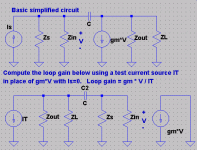
I see I've caused some confusion. I have no scanner, so I tried to describe the circuit in words. Bad idea!") . I tried sketching out the symbolic circuit with the LTSpice schematic capture and it came out okay. I've shown it below. My thought was not to model the circuit at a device level, but rather to have the simplest possible "macro model" (for lack of a better term) for whatever combination of devices are used in the Vas. My hope was to get a result simple enough that I could obtain some intuitive information from it. So the term "gm" I used is not the device-level transconductance, but rather the y21 value of the composite network. It's only equal to the device gm for a standard CE amp with no emitter resistor.
. I tried sketching out the symbolic circuit with the LTSpice schematic capture and it came out okay. I've shown it below. My thought was not to model the circuit at a device level, but rather to have the simplest possible "macro model" (for lack of a better term) for whatever combination of devices are used in the Vas. My hope was to get a result simple enough that I could obtain some intuitive information from it. So the term "gm" I used is not the device-level transconductance, but rather the y21 value of the composite network. It's only equal to the device gm for a standard CE amp with no emitter resistor.
I do realize that the circuit is very oversimplified, but what was important to me was the core ideas rather than ultimate accuracy.
Regarding the input impedance issue, you mentioned that the important thing was beta. But since hie=(beta + 1)*re, increasing beta has the effect of increasing the input impedance of a common emitter amplifier. So I think we're talking about the same thing, but just thinking about the problem in different ways.
You should be able to verify my loop gain expression using the circuit below.
I see I've caused some confusion. I have no scanner, so I tried to describe the circuit in words. Bad idea!
. I tried sketching out the symbolic circuit with the LTSpice schematic capture and it came out okay. I've shown it below. My thought was not to model the circuit at a device level, but rather to have the simplest possible "macro model" (for lack of a better term) for whatever combination of devices are used in the Vas. My hope was to get a result simple enough that I could obtain some intuitive information from it. So the term "gm" I used is not the device-level transconductance, but rather the y21 value of the composite network. It's only equal to the device gm for a standard CE amp with no emitter resistor.I do realize that the circuit is very oversimplified, but what was important to me was the core ideas rather than ultimate accuracy.
Regarding the input impedance issue, you mentioned that the important thing was beta. But since hie=(beta + 1)*re, increasing beta has the effect of increasing the input impedance of a common emitter amplifier. So I think we're talking about the same thing, but just thinking about the problem in different ways.
You should be able to verify my loop gain expression using the circuit below.
Attachments
About jcx'x post :
I was about to write a stupidity :
"The VAS input impedance is rather low here because no emitter resistor is used."
Then I checked in the Simulator. Remember the input diff stage + current mirror has an output impedance of about 100K (roughly...).
A simple transistor, and a cascoded transistor, both have an input Z of about 1K (Ic = 10mA, BC557C) at DC, falling first order after the dominant pole because of Cdom.
This 1K is small relative to the 100K so the "current source inptu stage" is valid.
However when using a super pair which has a lot more current gain, VAS input impedance raised to about 100K (which is about the same as the input stage output impedance, so it may be masking the real VAS impedance).
Conclusion : As we increase VAS gain, its input impedance increases too, and magnifies any nonlinearity in the input stage output impedance.
Does it matter ? I'm not sure really...
Yes, but in this case, if you model using voltage, can you tell me the output impedance of the input stage ? Not easy to calculate the output impedance of two collectors back-to-back...
I was about to write a stupidity :
"The VAS input impedance is rather low here because no emitter resistor is used."
Then I checked in the Simulator. Remember the input diff stage + current mirror has an output impedance of about 100K (roughly...).
A simple transistor, and a cascoded transistor, both have an input Z of about 1K (Ic = 10mA, BC557C) at DC, falling first order after the dominant pole because of Cdom.
This 1K is small relative to the 100K so the "current source inptu stage" is valid.
However when using a super pair which has a lot more current gain, VAS input impedance raised to about 100K (which is about the same as the input stage output impedance, so it may be masking the real VAS impedance).
Conclusion : As we increase VAS gain, its input impedance increases too, and magnifies any nonlinearity in the input stage output impedance.
Does it matter ? I'm not sure really...
jcx said:Gm is much more predictable for BJT than current gain and Gm based modeling shows commonality of operating principle with FETs where current gain is a fairly useless concept [/B]
Yes, but in this case, if you model using voltage, can you tell me the output impedance of the input stage ? Not easy to calculate the output impedance of two collectors back-to-back...
The level of sophistication is growing!
Why do you need dc feedback around the VAS amp?
I mean, are you trying to make this stage set the voltage gain of the system or are you intending to have global feedback do that?
According to Hugh the more feedback (as Cdom) the worse the thing sounds - so why apply even more feedback with a resistor?
What is the OL gain at DC ? It's actually impossible to answer this question, as it depends on so many parameters in the VAS, including transistor tempeartures, PCB insulation resistance, air hygrometry, DC leakage in Cdom... all of which can be signal-dependant.
Using a resistor would remove these uncertainties. Does it sound better ? I don't know. You'd gotta try.
Using a resistor would remove these uncertainties. Does it sound better ? I don't know. You'd gotta try.
A variant of the Hawksford cascode idea...
Since we were talking about the Hawksford cascode, I thought I'd mention an alternative that does a similar thing. I'd been playing around with simulations of distortion with the Hawksford cascode, and the distortion numbers looked very good. But the behavior of the amp in clipping was not good - it had a tendency to "bounce" off the rail rather than maintain a constant voltage in clipping. I tried using a Baker clamp to improve the clipping behavior, but it doesn't work right when integrated with the bias circuitry for the base of the common base amp. It ends up not working like a standard Baker clamp should, yet increases the distortion considerably as well.
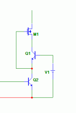
Then I remembered a circuit that Wyn Palmer of Analog Devices used in the AD846 op-amp. I've shown a variant below. I've represented the ampllifier's output stage as an unity gain VCVS. Assuming Q13 and Q9 are matched, the collector currents of Q13 and Q9 will be equal. The collector-base voltages of Q14 and Q10 are nearly equal but for a Vbe drop. So assuming Q14 and Q10 are matched, the instantaneous base currents of Q14 and Q10 are nearly equal. The "cloned" base current of Q10 gets injected into the emitter of Q10, which increases and linearizes the output impedance of Q10, while also making the composite circuit's current gain closer to unity.
The disadvantage of this circuit is of course the increased complexity and need to match devices. The advantage is that the base of Q10 is now at a fixed DC voltage. Assuming the bias voltage source for the base of Q10 can provide the instantaneous current necessary to pull it out of saturation quickly, clipping will be very clean. With the ideal voltage source V5, simulation shows the clipping behavior to be about as good as it gets. Simulated distortion numbers are nearly the same as the Hawksford cascode. So after endless experimenting with the simulator, I think I've finally found the topology I want to use for my amp!
Since we were talking about the Hawksford cascode, I thought I'd mention an alternative that does a similar thing. I'd been playing around with simulations of distortion with the Hawksford cascode, and the distortion numbers looked very good. But the behavior of the amp in clipping was not good - it had a tendency to "bounce" off the rail rather than maintain a constant voltage in clipping. I tried using a Baker clamp to improve the clipping behavior, but it doesn't work right when integrated with the bias circuitry for the base of the common base amp. It ends up not working like a standard Baker clamp should, yet increases the distortion considerably as well.
Then I remembered a circuit that Wyn Palmer of Analog Devices used in the AD846 op-amp. I've shown a variant below. I've represented the ampllifier's output stage as an unity gain VCVS. Assuming Q13 and Q9 are matched, the collector currents of Q13 and Q9 will be equal. The collector-base voltages of Q14 and Q10 are nearly equal but for a Vbe drop. So assuming Q14 and Q10 are matched, the instantaneous base currents of Q14 and Q10 are nearly equal. The "cloned" base current of Q10 gets injected into the emitter of Q10, which increases and linearizes the output impedance of Q10, while also making the composite circuit's current gain closer to unity.
The disadvantage of this circuit is of course the increased complexity and need to match devices. The advantage is that the base of Q10 is now at a fixed DC voltage. Assuming the bias voltage source for the base of Q10 can provide the instantaneous current necessary to pull it out of saturation quickly, clipping will be very clean. With the ideal voltage source V5, simulation shows the clipping behavior to be about as good as it gets. Simulated distortion numbers are nearly the same as the Hawksford cascode. So after endless experimenting with the simulator, I think I've finally found the topology I want to use for my amp!
Attachments
That was a nice idea. I just tried it out, and am having problems with bursts of parasitic oscillation on the large-signal sine wave output. I've seen this before with some of the more complex circuits from the Hawksford paper that contain super pairs - for example, the ones that jcx posted earlier in this thread a few months ago. I haven't been able to kill these with base stopper resistors so far. Interestingly, I can make the oscillations go away by switching from modified trapezoidal integration to Gear integration in LTSpice. I had the same experience with some of jcx's earlier examples as well.
I looked this up in Vladimirescu, and it seems that Gear has the effect of suppressing oscillations. He shows an example with a lossless LC circuit for which trapezoid gives the correct steady-state sine wave transient response, but Gear incorrectly shows a decaying sinusoid. Since Gear is incorrect in this case, I suspect that in practice the circuit may not be stable. Even with Gear enabled, when I drive the amp into clipping, the parasitic oscillations start immediately afterward. This circuit does show promise, since when using Gear and not clipping the amplifier, no oscillation appears and the distortion levels are about the same as the Hawksford cascode and the "Palmer cascode" that I posted earlier. (I don't know if Palmer invented this, it's just that the AD846 was the first place I saw it). I'm going to play around with this circuit some more and see if I can kill the oscillations with some other technique.
I looked this up in Vladimirescu, and it seems that Gear has the effect of suppressing oscillations. He shows an example with a lossless LC circuit for which trapezoid gives the correct steady-state sine wave transient response, but Gear incorrectly shows a decaying sinusoid. Since Gear is incorrect in this case, I suspect that in practice the circuit may not be stable. Even with Gear enabled, when I drive the amp into clipping, the parasitic oscillations start immediately afterward. This circuit does show promise, since when using Gear and not clipping the amplifier, no oscillation appears and the distortion levels are about the same as the Hawksford cascode and the "Palmer cascode" that I posted earlier. (I don't know if Palmer invented this, it's just that the AD846 was the first place I saw it). I'm going to play around with this circuit some more and see if I can kill the oscillations with some other technique.
andy,
I'm not certain that this arrangement nulls out the base current of Q10 in theory other than in a dc situation. Dynamically, the Cbc of Q14 will create a non-linear error current which is not cancelled. You could, I suppose, minimize this by cascoding Q14 at the expense of the gain modulation by Vce being different between Q10 and Q14.
It is also worth pointing out that the current gain of the "VAS" in this arrangement is half of that of a "VAS" without the Q13/Q14 circuit. So half the current gain is expended to null a base current at dc.
The absolute dc current gain of the "VAS" is not so important and varies all over the place anyhow with temperature and so on.
traderbam said:andy,
I'm not certain that this arrangement nulls out the base current of Q10 in theory other than in a dc situation. Dynamically, the Cbc of Q14 will create a non-linear error current which is not cancelled.
Not true. If you look carefully at the schematic, the collector of Q14 is bootstrapped to the amplifier output, not to a constant voltage. It swings one-for-one with the collector of Q14. So the total instantaneous collector-base voltage is different from that of Q10 by only one Vbe drop, even in an AC situation. If it did not track in this way, the simulated distortion reduction wouldn't be comparable to that of the Hawksford cascode, which works on basically the same principle - feedback of the instantaneous base current back to the emitter.
The high beta of the BC550C (typical ~600) seems to give enough current gain to reduce the distortion despite the factor of two beta reduction from the parallel connection. I did try adding an emitter-follower to the circuit inside the Miller feedback loop to increase the current gain, but it did not have much effect on the distortion. In the circuit with an ideal output stage, all harmonics except the second are below -120 dB with an output voltage swing equivalent to an output power of 300 Watts into 8 Ohms. This is with a very low unity loop-gain frequency of about 110 kHz, chosen to give clean square wave response into a 2 uF load capacitor. This gives only about 14 dB of global feedback at 20 kHz (where I computed the distortion). So I'm happy at this point to get a good combination of clean transient response and low harmonic distortion.
In the circuit with an ideal output stage
IMHO you'll really need an eitter follower with a "real world" output stage, whose input impedance varies a lot in the crossoevr region...
You've still got to thermally couple your transistor pairs...
Not true. If you look carefully at the schematic, the collector of Q14 is bootstrapped to the amplifier output, not to a constant voltage. It swings one-for-one with the collector of Q14. So the total instantaneous collector-base voltage is different from that of Q10 by only one Vbe drop, even in an AC situation.
Yes I understood this. This isn't my point. Consider the current path through the Ccb of Q10 and Q14 when the output voltage changes. Where do these currents flow? It is the difference in these two current paths that causes the asymmetry, not whether Vbes are matched or not.
Did Hawksford miss this?
peufeu said:
IMHO you'll really need an emitter follower with a "real world" output stage, whose input impedance varies a lot in the crossover region...
You've still got to thermally couple your transistor pairs...
Yes, certainly. My purpose with this simulation was to evaluate the contribution of the Vas to the distortion of the overall amp, neglecting the output stage distortion and nonlinear Vas loading. In other words, asking the question "how well can I do with a Vas having a perfect load?". Then proceeding to the next step, asking "how close to this ideal can I get with real-world drivers?". Putting a real output stage here would swamp out the contribution of the Vas distortion to the total amplifier distortion. I'm trying to take this one step at a time.
And with the shunt regulator for the output stage, the Vcb's of Q10 and Q14 will be off by several volts, rather than the single Vbe drop of the ideal case. But clean clipping is more important to me than getting the best possible distortion cancellation from Vcb matching.
As an aside, I'll be using MOSFET drivers as well as a MOSFET output stage like the Holton AV800, so the nonlinear load impedance on the Vas is dominated by the voltage-variable input capacitance of the MOSFET drivers. Drivers will be Fairchild FQP3N25 N-channel and FQP2P25 P-channel. Output devices will be paralleled Fairchild SFH9250L and Fairchild IRFP250B. Feedback for the Miller capacitor will not be from the Vas collector, but from the sources of the FET drivers. I tried connecting the Miller feedback to the amplifier outputs, but got degraded square wave response with capacitive loads (lots of ringing).
I have simulated the distortion with the drivers hooked up, driving the output stage and an ideal unity gain VCVS, with the overall feedback taken from the VCVS output rather than the FET output stage. The purpose of this was to evaluate the effect of nonlinear loading of the Vas, but neglect crossover distortion. I was rather surprised to find that the FETs yielded lower simulated distortion here at 20 kHz full power than loading with MJE340/MJE350 bipolar drivers.
traderbam said:
(...)Consider the current path through the Ccb of Q10 and Q14 when the output voltage changes. Where do these currents flow? It is the difference in these two current paths that causes the asymmetry, not whether Vbes are matched or not.
Did Hawksford miss this?
I didn't say anything about Vbe matching. What I was referring to is collector-base voltage (Vcb) matching. This addresses your point. The collector-base capacitance is part of a non-ideal (voltage-variable) collector-base impedance. When the output voltage varies, there will be non-ideal base currents from this (to answer the "where do the currents flow" question). If the compensation transistor is matched to the transistor it's compensating and the instantaneous collector-base voltages of the two devices match, then those non-ideal base currents will be the same between the compensating transistor and the transistor being compensated. This compensation current is fed back to the emitter of the transistor, cancelling its distorted base current. The compensation current includes the effect of non-linear collector-base capacitance because the Ccb current ends up as a component of the total instantaneous base current.
If you like, shoot me an email and I will send you Hawksford's description of this. You'll see in his paper that his technique helps neutralize the effect of non-ideal collector-base impedance. He did not miss this. If you still don't believe it, try simulating the distortion at high frequencies with a normal and Hawksford cascode. I'm doing this at 20 kHz, 69.3 Volts peak. If your assertion that the technique only works at DC were true, then distortion improvement would only occur at low frequencies. In fact, the technique achieves excellent large-signal high-frequency distortion reduction. This wouldn't be possible if it didn't take into account the non-linear collector-base capacitance.
Cascoding alone is a big step forward because the parasitic currents flowing through Cbc are not magnified by Miller effect anymore.
Question 1 : is it worth to fix the base current of the cascode, given that it'll only bring an improvement Beta times smaller than fixing the base current of the VAS transistor, which is done by simple cascoding ?
Question 2 : You should do the same for the upper current source feeding the VAS if you want to be coherent. Will you ?
Question 3 : if the VAS cascode Cbc variations match the current source cascode variations, it might fix it by itself. I wonder what is the matching between NPN and PNP transistors on this. There must be some cancellation, even if not as good as with your idea.
Question 4 : what about the VAS buffer transistor's Cbc variations ? Will you use a super pair ?
Question 5 : what about the attached schematic ? oops, I think it's wrong... but we could implement the Hawksford with a JFET or something (on low-voltage amps like headphone amps)
All Cbc variations, from the two cascodes and the VAS buffer, have the same "weight" here.
Attachments
Cascoding alone is a big step forward because the parasitic currents flowing through Cbc are not magnified by Miller effect anymore.
Yes, I agree.
Question 1 : is it worth to fix the base current of the cascode, given that it'll only bring an improvement Beta times smaller than fixing the base current of the VAS transistor, which is done by simple cascoding ?
Whether it's worthwhile to do this depends on priorities I guess. Here's some data comparing distortion at 69.3 Volts peak at 20 kHz with my circuit. The even harmonics don't seem to be affected much, but the odds are improved by 12-15 dB. For me it's worth it, though the change isn't as much of an improvement as I saw in my simulation of a fully complementary amplifier.
Uncompensated (dBc)
2nd: -95.2
3rd -110.3
4th -128.3
5th -122.7
6th -147.1
7th -138.6
Compensated (dBc)
2nd: -95.2
3rd -125.5
4th -129.6
5th -134.8
6th -148.2
7th -151.9
Question 2 : You should do the same for the upper current source feeding the VAS if you want to be coherent. Will you ?
Yes, that's what the figures above represent. One observation - I get symmetrical slew rates with this configuration. I'm now suspecting that the asymmetrical slew rates observed by Self for the single-ended design are a side effect of the type of constant current load he used for the Vas. The symmetrical slew rate was a pleasant surprise. I haven't checked the normal cascode for symmetrical slew rates yet.
Question 3 : if the VAS cascode Cbc variations match the current source cascode variations, it might fix it by itself. I wonder what is the matching between NPN and PNP transistors on this. There must be some cancellation, even if not as good as with your idea.
I agree with this also. The Cbc of the PNP will increase when the Cbc of the NPN decreases and vice versa, giving a more constant capacitance with voltage. I'm not quite sure how to isolate this effect in simulation though.
Question 4 : what about the VAS buffer transistor's Cbc variations ? Will you use a super pair ?
As I mentioned in post #296, I'm using common-drain MOSFETs for the Vas buffer and output stage, like the Holton AV800. Unfortunately, it appears that Anthony has removed the PDF file containing the schematic of this amplifier, so I can't provide a link. Your question brought up an interesting issue with the SPICE models of MOSFETs though. The gate-drain capacitance with the Level 1, 2 and 3 MOSFETs is modeled as being constant with gate-drain voltage, contrary to the data sheet! I verified this both with simulation and by looking up the formulas in Massobrio and Antognetti. The gate-drain capacitance is given by Cgd = Cgd0 * W, independent of Vgd. This is very inaccurate. I'm now looking into the LTSpice-specific VDMOS model for vertical MOSFETs. This model has a variable gate-drain capacitance. If it's not too difficult, I'm going to try to fit the parameters of this model to the MOSFET data sheets I have.
This also suggests the possibility of bootstrapping the Vas buffer drains (collectors) to the output voltage to cancel out the effects of variable capacitance as the gate-drain (collector-base) voltage varies. So far, the only circuits I've tried for this have had degraded transient response from their non-bootstrapped counterparts.
Question 5 : what about the attached schematic ? oops, I think it's wrong... but we could implement the Hawksford with a JFET or something (on low-voltage amps like headphone amps)
That looks like an interesting idea for low-voltage designs. The circuit I'm designing now is for +/-90 Volt rails, so the JFET idea can't be used.
All Cbc variations, from the two cascodes and the VAS buffer, have the same "weight" here.
Yes. That's why I'm now reconsidering the idea of bootstrapping the Vas buffer drains to the output voltage. I'm hoping I can come up with a circuit that does this without sacrificing the clean transient response I was getting with simple common-drain drivers.
I did some simulations for you, taking the problem in reverse. I have built CCS'es, change their collector voltage, and measure the current variations :
Circuits are : normal cascode, cascode-less, super-pair-cascode, and your circuit.
Results : we inject a voltage at the node between the two VAS collectors (10 kHz) and look at what happens.
Topmost graph shown the two collector currents for cascoded, middle graph for Normal.
Interesting point : the Cbc don't compensate as I said, actually it's the reverse ! The effects add up : when one CCS gives more current, the other draws less.
Bottom graph is error current going through the ficticious 0 ohm resistor I put at each VAS node (we want this to be 0 ideally).
Here's a closeup on the error current :
What do we see :
- Apparently PNP and NPN transistors are absolutely not matched regarding Cbc
- Cascode is a vast improvement over Normal
- Your circuit (codenamed "funky") is a vast improvement over Cascode
- A Baxandall Super Pair is even better, but it makes the simulator oscillate. However I don't think these will happen in real life, as the period of oscillations is exactly 4 simulation samples no matter what sample time I use... Therefore I postulate it's an artifact.
Thus I still doubt your circuit could be better than a Super Pair, besides something worries me :
How can you be sure the two transistors equally share their base current ? I know, the emitter degeneration resistors play a role...
What do you think ? I'm trying to be constructive, not just bashing your design...
An externally hosted image should be here but it was not working when we last tested it.
Circuits are : normal cascode, cascode-less, super-pair-cascode, and your circuit.
Results : we inject a voltage at the node between the two VAS collectors (10 kHz) and look at what happens.
Topmost graph shown the two collector currents for cascoded, middle graph for Normal.
Interesting point : the Cbc don't compensate as I said, actually it's the reverse ! The effects add up : when one CCS gives more current, the other draws less.
Bottom graph is error current going through the ficticious 0 ohm resistor I put at each VAS node (we want this to be 0 ideally).
An externally hosted image should be here but it was not working when we last tested it.
Here's a closeup on the error current :
An externally hosted image should be here but it was not working when we last tested it.
What do we see :
- Apparently PNP and NPN transistors are absolutely not matched regarding Cbc
- Cascode is a vast improvement over Normal
- Your circuit (codenamed "funky") is a vast improvement over Cascode
- A Baxandall Super Pair is even better, but it makes the simulator oscillate. However I don't think these will happen in real life, as the period of oscillations is exactly 4 simulation samples no matter what sample time I use... Therefore I postulate it's an artifact.
Thus I still doubt your circuit could be better than a Super Pair, besides something worries me :
How can you be sure the two transistors equally share their base current ? I know, the emitter degeneration resistors play a role...
What do you think ? I'm trying to be constructive, not just bashing your design...
- Status
- This old topic is closed. If you want to reopen this topic, contact a moderator using the "Report Post" button.
- Home
- Amplifiers
- Solid State
- Amplifier topology subjective effects