Hi,
Resistor in series with the LTP tail :
http://www.diyaudio.com/forums/soli...-self-wants-your-opinions-13.html#post3418023
Thanks forr,
Doug does indeed seem to dislike the presence of the LTP tail resistor.
His main concern seems to be how it will affect the functioning of the amplifier when the amplifier is being gradually brought up in rail voltage with a Variac. He points out that the LTP will not function normally until the rail has gotten up to a bit more than the voltage drop that we would have across the tail resistor in normal operation. Until that voltage is reached, the tail current source will be in saturation and the tail current will be eseentially established by the value of that LTP tail resistor.
My response to that is that it is fine to have that resistor in the design and that if you are concerned about it during laboratory bringing up of the supplies with a variac you can just short it out for those occasions.
I should probably not say this, as some may deem me careless, but I do not bring my amplifiers up the first time with a Variac anyway. I have not lost any amps doing it my way. I will sometimes bring the amp up the first time without the output stage connected and with the NFB tapped off of a center tap of the driver transistor to make sure the front-end is right.
BTW, whenever I have an amplifier that has +/-15V available anyway, I tend to run the LTP tail current source from the -15V supply.
Cheers,
Bob
Another resistor that I hope Doug gets rid of is the one in series with the base of the controlling transistor in his amplified negative feedback current sources.Thanks forr,
Doug does indeed seem to dislike the presence of the LTP tail resistor.
This resistor needlessley reduces the loop gain local to the current source and brings no compensating benefits.
Another resistor that I hope Doug gets rid of is the one in series with the base of the controlling transistor in his amplified negative feedback current sources.
This resistor needlessley reduces the loop gain local to the current source and brings no compensating benefits.
Hi Mike,
Any chance he's worried about somehow burning out the controlling transistor if by some way the current in the VAS transistor greatly exceeds the design value, putting a really large amount of current into the base? Seems like an unlikely fault condition, though.
I also wonder if it is intended to tame some perceived stability issue by allowing Miller capacitance in the Ccb of the controlling transistor to add a pole that tames HF loop gain a bit.
Cheers,
Bob
I also wonder if it is intended to tame some perceived stability issue by allowing Miller capacitance in the Ccb of the controlling transistor to add a pole that tames HF loop gain a bit.
The intention is to prevent "parasitic" oscillation. Whether this is actually oscillation due to a negative-feedback instability or more like the sort of oscillations seen with cascodes or emitter-follower output stages, I'm not sure. For the former, presumably the loop should really be probed with a Middlebrook probe to assess stability of the feedback loop?
Nonlinear distortion creates new frequencies, linear distortion does not. Nonlinear distortion involves a nonlinear transfer curve.
Distorsion is by the definition creation of new frequencies ,
be it HD , IMD , PID , SID and whatever acronym that as an
actual meaning mathematicaly speaking.
Hi Mike,
Any chance he's worried about somehow burning out the controlling transistor if by some way the current in the VAS transistor greatly exceeds the design value, putting a really large amount of current into the base? Seems like an unlikely fault condition, though.
I also wonder if it is intended to tame some perceived stability issue by allowing Miller capacitance in the Ccb of the controlling transistor to add a pole that tames HF loop gain a bit.
Cheers,
Bob
The intention is to prevent "parasitic" oscillation. Whether this is actually oscillation due to a negative-feedback instability or more like the sort of oscillations seen with cascodes or emitter-follower output stages, I'm not sure. For the former, presumably the loop should really be probed with a Middlebrook probe to assess stability of the feedback loop?
Bob, I suspect this resistor was used by Self to protect the control transistor in the event of the current source transistor failing short circuit. This is exceedingly unlikely.
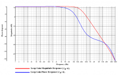
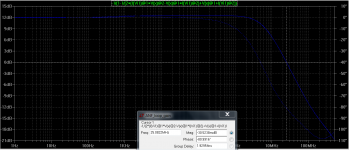
Harry, I doubt that the amplified negative feedback (ANF) current source could be a source of instability; its loop gain barely exceeds 10 db, and, moreover, its phase margin exceeds 90 degrees at a unity loop gain frequency of only 500KHz. See figure below.
Attachments
Last edited:
Bob,.... consider adding Monte Carlo analysis DETAILS to your next revision, plus supporting component models.
"Thou shall run a Monte Carlo analysis on every circuit," has become one of my design commandments.
"Monte Carlo" is not in the appendix of your current book. Classical Monte Carlo LTSpice simulation techniques are important for any circuit design, including how to create the device models required for statistical simulation.
I have an amplifier PCB for complementary differential inputs which supports complementary current mirror loads on the LTPs, as well as just resistor loads as common in early Krell-type topologies. The amp with just resistor LTP loads is very tolerant of component selection variations. If I hand match the transistors for the complementary current mirror load topology it produces exceptionally low THD and wide BW. When a different grade bipolar transistor is mixed in, the amps with complementary current mirror loads have 20x higher THD, and additional R+C serial filters across the LTP tails are required to avoid oscillation. i.e. lower BW is necessary to support wide transistor specs. A basic LTSpice Monte Carlo analysis using your transistor models never converges for the complementary current mirror load topology.
Bob, I suspect this resistor was used by Self to protect the control transistor in the event of the current source transistor failing short circuit. This is exceedingly unlikely.
Harry, I doubt that the amplified negative feedback (ANF) current source could be a source of instability; its loop gain barely exceeds 10 db, and, moreover, its phase margin exceeds 90 degrees at a unity loop gain frequency of only 500KHz. See figure below.
Hi Mike,
It seems like there must be something wrong with the loop gain analysis whose results you posted. I'm guessing loop gain is way higher. Your plot shows loop gain only about 10dB at DC. with with low-frequency hand-waiving we can estimate what the loop gain might be.
For the loop, the main current source transistor acts like an emitter follower. The control transistor acts like a common emitter stage. We can assume that the operating current sourced into the collector of the control transistor comes from a current source. Assume that is 1mA. This sets the gm of the control transistor at 40mS.
Assume the main transistor is set for 10mA and has a 60 ohm emitter resistor. Assume current gain of that transistor is 100. Impedance at its base is then 6000 ohms. Loop gain is the gain of the common-emitter control transistor stage, which is gm*RL, which is 40mS * 6k = 240 ~48dB.
Cheers,
Bob
Bob, I suspect this resistor was used by Self to protect the control transistor in the event of the current source transistor failing short circuit.
I think Self says (where ?) that this resistor is for debugging purposes in case of failure.
Hi Mike,
It seems like there must be something wrong with the loop gain analysis whose results you posted. I'm guessing loop gain is way higher. Your plot shows loop gain only about 10dB at DC. with with low-frequency hand-waiving we can estimate what the loop gain might be.
For the loop, the main current source transistor acts like an emitter follower. The control transistor acts like a common emitter stage. We can assume that the operating current sourced into the collector of the control transistor comes from a current source. Assume that is 1mA. This sets the gm of the control transistor at 40mS.
Assume the main transistor is set for 10mA and has a 60 ohm emitter resistor. Assume current gain of that transistor is 100. Impedance at its base is then 6000 ohms. Loop gain is the gain of the common-emitter control transistor stage, which is gm*RL, which is 40mS * 6k = 240 ~48dB.
Cheers,
Bob
Hi Bob,
I simulated the loop gain of the ANF current source circa 2004 for an unpublished 103pg article I wrote on double pole compensation and the push-pull TIS.
I simply used the Adel S. Sedra and Kenneth C. Smith (to be found in their book "Microelectronic circuits") method of measuring loop gain in SIMetrix.
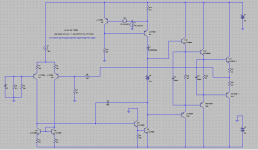
Similarly, you can measure the ANF current source's loop gain in LTSpice by placing the so-called "Tian" loop gain probe (which is really a Middlebrook probe) in series with the base of the control transistor and decoupling the current source transistor from the collector of the TIS in a Thompson topology amplifier by means of a very large inductor. The results are shown below.
In this case the loop gain is of the order of 12dB and phase margin is 100degrees at unity loop gain frequency of roughly 25MHz. Note that loop gain increases slightly as the reference resistor, to which the current source's base is connected, is reduced in value; the unity loop gain frequency also increases. It is not immediately apparent, to me anyway, why this is the case.
I have attached the asc and the relevant models for those interested in running the simulation.
Unless you can point out shortcomings with this approach I believe my results are correct. P.S. where did you get that 6K value from?

Attachments
Last edited:
Bob,.... consider adding Monte Carlo analysis DETAILS to your next revision, plus supporting component models.
"Thou shall run a Monte Carlo analysis on every circuit," has become one of my design commandments.
"Monte Carlo" is not in the appendix of your current book. Classical Monte Carlo LTSpice simulation techniques are important for any circuit design, including how to create the device models required for statistical simulation.
I have an amplifier PCB for complementary differential inputs which supports complementary current mirror loads on the LTPs, as well as just resistor loads as common in early Krell-type topologies. The amp with just resistor LTP loads is very tolerant of component selection variations. If I hand match the transistors for the complementary current mirror load topology it produces exceptionally low THD and wide BW. When a different grade bipolar transistor is mixed in, the amps with complementary current mirror loads have 20x higher THD, and additional R+C serial filters across the LTP tails are required to avoid oscillation. i.e. lower BW is necessary to support wide transistor specs. A basic LTSpice Monte Carlo analysis using your transistor models never converges for the complementary current mirror load topology.
Hi Linesource,
That's a pretty tall order.
The amplifier you are referring to with the complementary current mirror loads - is that the Slone topology that basically does not work? Or am I misunderstanding the topology you are referring to. Can you post a schematic of it or just the IPS-VAS portion? Having to match transistors to get stable performance is a dead giveaway of a problematic circuit.
That Monte Carlo analysis that you mentioned that does not converge with my models - does it converge with manufacturer's models? I'm not sure whether you are saying this is a reflection on my models or on the circuit.
Cheers,
Bob
Hi Bob,
Help Me! I have become addicted to Monte Carlo gambling")
1) I use the "improved" aka "buffered Widlar" current mirror topology, plus a 47K ohm feedback resistor across the LTP to assure correct start-up for complementary input mirrors.
2) The Monte Carlo analysis will converage with a few transistor models (like MAT02, MAT03), but not with your BC550 BC560 models or the LTSpice BCxxx models. The Monte Carlo will not pass if I swap one BC550A in place of one BC550C.
3) Passing a Monte Carlo analysis with a complementary current mirror input with your models is possible if a "serious" R+C series filter is placed across the LTP, and the TMC feedback is adjusted for -3db ~200Khz BW. A "nominal" simulation runs with a >1Mhz -3db point.
4) A Monte Carlo analysis will easily pass for a complementary input topology with just resistor loads in the LTP. I understand why my Krell KMA100s used such a simple circuit topology in 1985.
For the physical prototype I hand matched all transistors, and the real amplifier has been running for almost 1 year without self-destruction. I decided to run Monte Carlo before building several copies, and adding protection circuits.
I suspect that most amplifier designs discussed here would require substantial redesign before they could pass a robust Monte Carlo sim.
Help Me! I have become addicted to Monte Carlo gambling
1) I use the "improved" aka "buffered Widlar" current mirror topology, plus a 47K ohm feedback resistor across the LTP to assure correct start-up for complementary input mirrors.
2) The Monte Carlo analysis will converage with a few transistor models (like MAT02, MAT03), but not with your BC550 BC560 models or the LTSpice BCxxx models. The Monte Carlo will not pass if I swap one BC550A in place of one BC550C.
3) Passing a Monte Carlo analysis with a complementary current mirror input with your models is possible if a "serious" R+C series filter is placed across the LTP, and the TMC feedback is adjusted for -3db ~200Khz BW. A "nominal" simulation runs with a >1Mhz -3db point.
4) A Monte Carlo analysis will easily pass for a complementary input topology with just resistor loads in the LTP. I understand why my Krell KMA100s used such a simple circuit topology in 1985.
For the physical prototype I hand matched all transistors, and the real amplifier has been running for almost 1 year without self-destruction. I decided to run Monte Carlo before building several copies, and adding protection circuits.
I suspect that most amplifier designs discussed here would require substantial redesign before they could pass a robust Monte Carlo sim.
Hi Bob,
I simulated the loop gain of the ANF current source circa 2004 for an unpublished 103pg article I wrote on double pole compensation and the push-pull TIS.
I simply used the Adel S. Sedra and Kenneth C. Smith (to be found in their book "Microelectronic circuits") method of measuring loop gain in SIMetrix.
Similarly, you can measure the ANF current source's loop gain in LTSpice by placing the so-called "Tian" loop gain probe (which is really a Middlebrook probe) in series with the base of the control transistor and decoupling the current source transistor from the collector of the TIS in a Thompson topology amplifier by means of a very large inductor. The results are shown below.
In this case the loop gain is of the order of 12dB and phase margin is 100degrees at unity loop gain frequency of roughly 25MHz. Note that loop gain increases slightly as the reference resistor, to which the current source's base is connected, is reduced in value; the unity loop gain frequency also increases. It is not immediately apparent, to me anyway, why this is the case.
I have attached the asc and the relevant models for those interested in running the simulation.
Unless you can point out shortcomings with this approach I believe my results are correct. P.S. where did you get that 6K value from?
Hi Mike,
Your problem appears to be the use of the very large inductor. It does not allow the current source transistor to function normally. The inductor is superfluous to the simulation anyway.
This sort of thing is why we always want to be able to do a simple sanity check on our results.
The 6k is simply the approximate input resistance as seen at the base of the current source transistor - it is the 60-ohm RE multiplied by the transistor's beta of 100. It is the dominant load for the common-emitter configured control transistor.
Let me know if there is something you think is wrong with my simple loop gain analysis.
Cheers,
Bob
Hi Bob,
Help Me! I have become addicted to Monte Carlo gambling
1) I use the "improved" aka "buffered Widlar" current mirror topology, plus a 47K ohm feedback resistor across the LTP to assure correct start-up for complementary input mirrors.
2) The Monte Carlo analysis will converage with a few transistor models (like MAT02, MAT03), but not with your BC550 BC560 models or the LTSpice BCxxx models. The Monte Carlo will not pass if I swap one BC550A in place of one BC550C.
3) Passing a Monte Carlo analysis with a complementary current mirror input with your models is possible if a "serious" R+C series filter is placed across the LTP, and the TMC feedback is adjusted for -3db ~200Khz BW. A "nominal" simulation runs with a >1Mhz -3db point.
4) A Monte Carlo analysis will easily pass for a complementary input topology with just resistor loads in the LTP. I understand why my Krell KMA100s used such a simple circuit topology in 1985.
For the physical prototype I hand matched all transistors, and the real amplifier has been running for almost 1 year without self-destruction. I decided to run Monte Carlo before building several copies, and adding protection circuits.
I suspect that most amplifier designs discussed here would require substantial redesign before they could pass a robust Monte Carlo sim.
Hi Linesource,
It sounds like the design you are talking about is like the circuit I show in Figure 7.10 in my book. Is that correct?
In your circuit implementation, are you using the twin Miller feedback compensation capacitors shown in Figure 7.10? It sounds like your amplifier has a high frequency stability problem.
Although Monte Carlo can be useful in finding weaknesses in a design for certain combinations of component variations, it is important that the design be robust by design before doing a Monte Carlo. This certainly includes matters of feedback stability, but also includes design choices that keep sensitivity of the circuit behavior to various components to a reasonable value. For example, a circuit design whose behavior and performance depends highly on transistor beta may not even be worth doing a Monte Carlo on - why do that when you should know up-front that the circuit is not robust to the variations that it will be subjected to in the Monte Carlo?
Cheers,
Bob
Hi Mike,
Your problem appears to be the use of the very large inductor. It does not allow the current source transistor to function normally. The inductor is superfluous to the simulation anyway.
This sort of thing is why we always want to be able to do a simple sanity check on our results.
The 6k is simply the approximate input resistance as seen at the base of the current source transistor - it is the 60-ohm RE multiplied by the transistor's beta of 100. It is the dominant load for the common-emitter configured control transistor.
Let me know if there is something you think is wrong with my simple loop gain analysis.
Cheers,
Bob
Bob, the inductor is not a problem. It is required to isolate the current source from the singularities of the rest of the circuit so that only the loop gain and the singularities local to the current source can be ascertained.
The input resistance or impedance at the input of the current source BJT is not 6K: it is more like 6k in parallel with the resistor delivering current to both the control transistor's collector and the source's base.
Mike, with regard to the 6k, you are right, but note that in my simple analysis I stated that the current to run the control transistor was a current source.
You need to run the current source in isolation. You do not need to run it inside an amplifier to analyze whether such a current source has a certain amount of loop gain. We are just talking about a 2-transistor circuit here. Get rid of the inductor and just run the current source by itself, with the output of the current source connected to the supply or though a resistor of reasonable size to the supply.
In the approach you are using, you are basically loading the current source with a current source, which is what the huge inductor is at AC. We don't test current sources by loading them with a current source.
Cheers,
Bob
The inductor greatly increases the impedance at the CCS collector, increasing the magnification of its miller capacitance and Early effect. What you need to give it is a voltage source+resistor at the collector, not a high-impedance load. This is what will emulate isolation, not an inductor.
Mike, with regard to the 6k, you are right, but note that in my simple analysis I stated that the current to run the control transistor was a current source.
Using a current source, as you did in your analysis, is unrealistic and probably explains your somewhat exaggerated loop gain result. I used a more realistic resistor.
You need to run the current source in isolation. You do not need to run it inside an amplifier to analyze whether such a current source has a certain amount of loop gain. We are just talking about a 2-transistor circuit here. Get rid of the inductor and just run the current source by itself, with the output of the current source connected to the supply or though a resistor of reasonable size to the supply.
In the approach you are using, you are basically loading the current source with a current source, which is what the huge inductor is at AC. We don't test current sources by loading them with a current source.
Cheers,
Bob
Running the current source in isolation is precisely what I am doing by isolating it from the rest of the circuit with a very large inductor. The use of a large inductor for this purpose is routinely recommended by such luminaries as Rosenstark, Sedra and Smith.
You cannot obtain valid results by simply connecting the current source to a voltage source via a resistor because that resistor would define the output impedance of the current source giving wildly inaccurate results.
I have never heard of an inductor being described as a current source by anyone; it is no such thing.
Rather, the inductor is a virtual open circuit at all frequencies of interest allowing the output impedance of the current source to be defined solely by the output impedance of the source BJT.
Last edited:
The inductor greatly increases the impedance at the CCS collector, increasing the magnification of its miller capacitance and Early effect. What you need to give it is a voltage source+resistor at the collector, not a high-impedance load. This is what will emulate isolation, not an inductor.
No. Read "Feedback Amplifier Principals" by Sol Rosenstark.
I have had a 2-Q CCS oscillate, and a 2-Q current mirror oscillate. So there is more to it than this.
With an inductor at the collector, open-loop gain will dramatically worsen due to the output transistor's Rin=Rm. A collector resistor effectively turns the output transistor into a C-B diode across the first transistor, regardless of static Vce. Measure Rm and Rin of the output transistor in your simulation. You'll find it's much different with and without an output inductor.
BTW, the feedback in that CCS is not at the output. Therefore Zout is paralleled by Zcb of the output transistor. It is analogous to putting a resistor in series with the output of any voltage amp.
- Home
- Amplifiers
- Solid State
- Bob Cordell's Power amplifier book