Probe
Hi Edmond,
I don't know if I can test with the dumy OPS today but surely tomorrow.
However I checked my probes. They are HAMEG HZ36 Probes
ratio 1:1 - 10MHz - 35ns - 1Mohm - 46pF
or switched into
ratio 10:1 - 150MHz - 2ns - 10Mohm - 18pF
Maybe this explains something?
Greetz
Olivier
Hi Edmond,
I don't know if I can test with the dumy OPS today but surely tomorrow.
However I checked my probes. They are HAMEG HZ36 Probes
ratio 1:1 - 10MHz - 35ns - 1Mohm - 46pF
or switched into
ratio 10:1 - 150MHz - 2ns - 10Mohm - 18pF
Maybe this explains something?
Greetz
Olivier
Hi Olivier,
According to a sim, 46pF has little effect on the phase response. So something else causes the large discrepancy between virtual and real life.
BTW, why R13, R14, R9b & R12b? Did Randy tell you to do so? Anyhow, just replace them by a short. I'm not saying that they are responsible for all the troubles, but they don't do any good either.
Cheers,
E.
Too Many R's
Hi Edmond,
You are right, Randy specifies those base resistors. On the other hand the emitter resistors in the regulating Q is my own brewery... No cheers for this one thus. This evening they will be replaced by shorts. Maybe I will need to adapt the regulated Q's emitter resistor to maintain the same tail current.
Edmond, do you think this phase response is linked to PCB or unmatched devices? I hear people breadboarding schematics with perfect results so I can hardly believe this is a problem here !?
Any clues?
Schol,
Olivier
Hi Edmond,
You are right, Randy specifies those base resistors. On the other hand the emitter resistors in the regulating Q is my own brewery... No cheers for this one thus. This evening they will be replaced by shorts. Maybe I will need to adapt the regulated Q's emitter resistor to maintain the same tail current.
Those emitter resistors have a negative impact on the stability of the tail currents, that is, it makes them more dependent on the supply voltage.
Edmond, do you think this phase response is linked to PCB or unmatched devices? I hear people breadboarding schematics with perfect results so I can hardly believe this is a problem here !?
Any clues?
Schol,
Olivier
Hi Olivier,
It's very unlikely that unmatched devices have anything to do with the phase response. It's either an error in your PCB, or a wrong component. Sometimes it even happens that a capacitor or resistor is stamped with a wrong value.
Cheers,
E.
Hi Edmond,
Yesterday I tried with the dummy OPS. I didn't have time to plot the points or to go through the spectrum but I measured 2 or 3 points and the results are almost identical to the previous test w/o OPS. There is surely some tolerance for read out but havinf the OPS didn't resolve the major difference between real and simulated.
Right now I removed and bridged the resistors in the emitter legs of the regulating Q's R9B and R12B (R13 & R14 are sill in place for the moment)
I will write my findings in a minute or so...
Do you think parasitic caps between tracks and planes on the PCB could be in cause? I know they impact performance in this regard but I can hardly believe it is so critical at under 1MHz...
Till L8ER
Olivier

>I am starting to get a bit discouraged
Not to discourage you even further, but this only the beginning. The development of the PGP, for example, took 6 month!
As a next step, I would check all DC currents and voltages whether in accordance with the sim.
How did you remove the cascodes? By removing Q15, Q16, R18, R19, the cascode bias stuff and putting jumpers in the appropriate pads?
Cheers,
E.
Analsys 7d
Good Evening Edmond,
I replaced the Cascode. R9B & R12B are bridged. The R13/R14 are still in place but I will remove them tomorrow for a try.
Just to have everything lined up here is the .CIR again As-Built Ver7d.
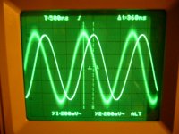
I plotted some extra points on the AC analyses too. There seem to be an interesing figure. Any clues to why it looks like that?
I also send you a picture of the scope trace at 550KHz Sine. The Gain is near 0 (1 dB or so). You can see the phase delay.
You can also see that the output trace is shifting up and down and makes it unclear. It looks like a sine wave with a very thick trace.
Is this normal ? Is this related to my phase problem or not?
Greetz
Olivier
Good Evening Edmond,
I replaced the Cascode. R9B & R12B are bridged. The R13/R14 are still in place but I will remove them tomorrow for a try.
Just to have everything lined up here is the .CIR again As-Built Ver7d.
I plotted some extra points on the AC analyses too. There seem to be an interesing figure. Any clues to why it looks like that?
I also send you a picture of the scope trace at 550KHz Sine. The Gain is near 0 (1 dB or so). You can see the phase delay.
You can also see that the output trace is shifting up and down and makes it unclear. It looks like a sine wave with a very thick trace.
Is this normal ? Is this related to my phase problem or not?
Greetz
Olivier
Attachments
Edmond,
I did not read your post before i posted mine ...
I removed QCC1 and QCC2 and placed a bridge between Collector and Emitter. The rest was left in place.
As for the discouragement. At least it makes me accept that it is difficult and what I am going throug is 'normal'.
Tomorrow I will check every node voltage and every current where I can.
Good Night
Olivier
DC
Hi Edmond,
Hereby you find the measured nodevoltages of the schematic rev.7d.
I redrew the Bias Generator on the schematic since it is there in reality too. Just to have identically the same thing.
I noticed just two differences that attracted my attention. I guess the one between zeners is not important but the one on the signal input looks weird.
It is the same voltage as the DC offset at the output or at the Feedback input of the LTP... I will check out if there isn't a bridge or so between them...
Do you notice something strange appart from that?
I did not check if the voltage measured at the node indicated on the schematic by MC9 is present on all its termination points. This would indicate a plain PCB error... I will check this later...
Greetz
Olivier
Attachments
Edmond,
[snip]
I removed QCC1 and QCC2 and placed a bridge between Collector and Emitter. The rest was left in place.
[snip]
Olivier
Hi Olivier,
Of course, that's the easiest way. But in case you would decide to delete the cacodes definitely, you better delete the other trannies, because of the heat sink, which you can't move. (and modify some other component values to limit the dissipation of Q101 and Q102, or have these trannies a heat sink as well?)
Cheers,
E.
Cascode
Hi Edmond,
Yes I removed them the easy way just to see the behavior. Since I run on 50V rail only (for now) & the VAS Iq = 12mA the DC operating point dissipates 600mW which doesn't heat Q16 and Q15 too much working w/o Cascode. But anyway the Cascode is mounted back on the PCB.
Since I could not notice any difference...
Yes also Q101/Q102 has heatsinks (not really necessary).
I am trying to find schematic mods in MC9 to make the simulated response look like the real one. This could give me a hint on what's wrong ...
I think I got a pole way too low in freq which makes the phase drop too steeply. Then I got some zero's too making it go uo again followed by more poles making it dive again (these last poles are probably logic) ... it's the first pole together with those zero's that makes the difference ...
If you see any strange thing on the DC voltages as posted before please let me know ...
Greetz
Olivier
Edmond,
I meant the one where the input signal is attached. In the sim it shows 0V whereas in reality it measures -40mV.
Also the point between RFB3 & 4 shows -40mV whereas the sim shows -10p or ~0V.
But then again, if the source is removed it is very logical that these -40mV are measured since it is the same voltage as on the other side of RFB3 because this side is connected nowhere. With signalsource the simulator puts that node at 0V whereas in reality it remains -40mV... probably just a sim thinigy.
There is one thing I discovered. The CAP in the GFL is not 4700uF but 470uF ... I wouldn't be able to see the rest of the PCB if it were 4700uF")
But ... wat nu?
Olivier
I meant the one where the input signal is attached. In the sim it shows 0V whereas in reality it measures -40mV.
Also the point between RFB3 & 4 shows -40mV whereas the sim shows -10p or ~0V.
But then again, if the source is removed it is very logical that these -40mV are measured since it is the same voltage as on the other side of RFB3 because this side is connected nowhere. With signalsource the simulator puts that node at 0V whereas in reality it remains -40mV... probably just a sim thinigy.
There is one thing I discovered. The CAP in the GFL is not 4700uF but 470uF ... I wouldn't be able to see the rest of the PCB if it were 4700uF
But ... wat nu?
Olivier
Edmond,
I meant the one where the input signal is attached. In the sim it shows 0V whereas in reality it measures -40mV.
Hi Olivier,
This Vi node (the right side of RFB4) to which it is connected (or should be connected to) in reality? to the signal generator, right? Perhaps there is a cap in series with the signal generator's output. So, just measure the DC voltage right at the output of the signal generator. If it's 0V, then indeed something is wrong with the PCB.
Also the point between RFB3 & 4 shows -40mV whereas the sim shows -10p or ~0V.
But then again, if the source is removed it is very logical that these -40mV are measured since it is the same voltage as on the other side of RFB3 because this side is connected nowhere. With signalsource the simulator puts that node at 0V whereas in reality it remains -40mV... probably just a sim thinigy.
There is one thing I discovered. The CAP in the GFL is not 4700uF but 470uF ... I wouldn't be able to see the rest of the PCB if it were 4700uF
But ... wat nu?
Olivier
>The CAP in the GFL is not 4700uF but 470uF
Never mind.
Cheers,
E.
Last edited:
DC Testing
Hi Edmond,
Where the signal generator is connected to the circuit, that is just to the right of RFB4, the DC analyses on simulation indicates 0VDC.
In reality however I measured about -43mVDC. Admitted this is not a big difference but it struck me because some other important nodevoltages also are around 40mV as you can see on the DC-Analyses chart of previous posts.
So you asked me to measure the output probe of the signal generator only. Well, when it is connected we read 40mV, when released from the circuit but keeping my voltmeter still on the output probe the 40mV starts to fall slowly like a discharging cap finally reaching 0VDC. In other words the DC voltage on the output probe of the signal generator is 0VDC. The point on the PCB itslef is 40mV ... so indeed it looks like the signal generator has an output cap in series with it ....
What can you figure out of this??
if it is of any use : Sig Gen = METRIX GX310.
Bye & Cheers
Olivier
Next onset
Hi,
Here the latest implementation of the schematic & pcb for the amp i desperately want to build. The last version (before this one I working but not as i would like)
Main differences :
- PCB density much higher , pcb size is 40% of previous area due to smaller components (why use 500mW resistors while they dissipate only 10mW?). Main resistor set = 1/8 W, some are 1/4 W and a few are 1/2 W like feedback resistors, ...)
- The old pcb had optional components like both TMC & TPC compensation were implemented, with or without VBE multiplier (here is none since there is no ops and it's just proto to conlude ips and vas), all these extra stuff lengthen the traces and chances for parasites increase
- the famous link trace between ips and vas is kept as short as i could (still long i find, but ok this should do)
-the board is now 2 layer instead of 4 layer. I played with copper planes etc but this time i keep it simple. maybe 4L in 1.55mm FR4 thickness makes them be close to eachother especially those seperated only by a prepreg (?) something 200um. Crossing V rails like +70V and -70V separated with 200um FR4 might be close to arcing no? If not, at least influence eachother a lot.
Have a look
Attachments
update
Hello there,
Here is the update of the schematic, (pcb will come later as i need to redraw it from scratch).
It contains both the cap between bases of the darlington vases and the rc network between rail and ouput-ips/input-vas node. Real testing will show which one helps best. C17A/C17B or C12-R25/R27-C13. Or both systems together.
I removed the fuses just to keep the test pcb small
I added a simple bias circuit and a tiny ops. beware that the .cir circuit uses 2SA1381 Q whereas i will use 2SA1930 Q for them with heatsinks (larger pcb , ... , too bad ).
I am still not sure about the baker clamps around the vas. I know Edmond changed to another circuit once but ... now i am unsure. Same thing for the cmcl circuit there are two options , this is the initial one.
Anyway, these options should work.
Notice C14 is optional idem for R19, C9, R36, R37, R44, R43.
More optionals than i wanted but ok, they are not causing tracks to become much longer.
I will create the pcb layout as small as possible. Will use 1.25mm tracks with 1.5mm spacing constraint.
Will be back l8er with more news
cheers
olivier
Attachments
Hi,
Here a pdf version of my schematic and pcb version.
Feel free to comment...
Greetz,
Olivier
Hi Olivier,
Is this the latest version of the PCB?
BTW, please wait with modifying the front-end, as I have more in petto:
With a full fledged OPS the Miller loop behaves quite different.
Long story short story, no need to increase the time constants of the lead-lag compensation at the VAS input that much (330pf & 15 Ohms). 150pF & 33 Ohms will do just fine.
A few more questions: Did you already order the PCBs for the OPS, or are you still in the design phase?
Is the PSU voltage really that high: 75V?
Cheers,
E.
- Status
- This old topic is closed. If you want to reopen this topic, contact a moderator using the "Report Post" button.
- Home
- Amplifiers
- Solid State
- HEEEELLLPPP : M. Randy Slone Mirror Image Topology Construction - Troubles