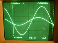
What is this?
With the amp completely powered down and w/o input signal I still measure about 20-30mV of noise signal with a base period of 600KHZ with 13MHZ modulated on top as well as RF components ... I worry less about the MHZ's and RF's but what about that 600KHZ ? It is within the amplifying bandwidth of the amplifier ... should I take care of this or is it just an irelevant artifact ?
Thnx
Olivier
Edmond,
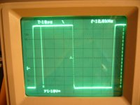
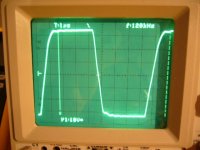
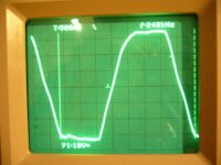
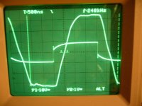
Just for a better reading here are some pictures of the latest situation with the dummy OPS connected.
The pictures are as follows :
12KHZ SQW output
120KHZ SQW output
240KHZ SQW output
240KHZ SQW input & output (dual)
Idem but Sine wave
And one with no input signal applied and even no powersupply to the amp.
I also send the PCB top component layer
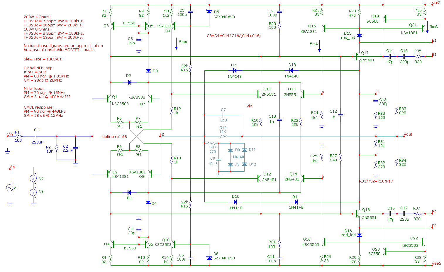
+ schematic as built now (with ops) pdf + cir(txt) file
If you want the PCB layer PDF's I can send them too but i need to find some way to make it smaller (it is 5MB now and cannot be uploaded here)
Cheers
Olivier
Just for a better reading here are some pictures of the latest situation with the dummy OPS connected.
The pictures are as follows :
12KHZ SQW output
120KHZ SQW output
240KHZ SQW output
240KHZ SQW input & output (dual)
Idem but Sine wave
And one with no input signal applied and even no powersupply to the amp.
I also send the PCB top component layer
+ schematic as built now (with ops) pdf + cir(txt) file
If you want the PCB layer PDF's I can send them too but i need to find some way to make it smaller (it is 5MB now and cannot be uploaded here)
Cheers
Olivier
Attachments
-
 P1040969.JPG102.3 KB · Views: 282
 -
 P1040970.JPG92 KB · Views: 270
 -
 P1040971.JPG98.8 KB · Views: 264
 -
 P1040972.JPG92.1 KB · Views: 260
 -
 P1040975.JPG100.1 KB · Views: 254
 -
 P1040976.JPG98.6 KB · Views: 58
 -
CMCL_20_TMC&TPC_AsBuilt4.cir.txt96.4 KB · Views: 63
-
CMCL_20_TMC&TPC_AsBuilt4_PCB_TOP.pdf44 KB · Views: 71
-
CMCL_20_TMC&TPC_AsBuilt4.pdf23.8 KB · Views: 117
oliver, i put your schematic into circuit maker, it's got some major design flawsm you can not have 2 terminals of a transistor tied together and it work. order the free version and do the schematic in there and you'll see shat i'm talking about man. nice board layout by the way.
.......... it's got some major design flawsm you can not have 2 terminals of a transistor tied together and it work.
............
Which trannies? Do you mean Q5 ad Q8?
you can not have 2 terminals of a transistor tied together and it work.
 That depends on the function of the transistor. Base and emitter tied together makes a diode, collector and base tied together makes a current source, and used with another transistor, a current mirror like Q5 and Q8.
with shorts on q5 and q8 it'll never work
A 'degree' in electronics and 17 years of 'experience'. Yet, never heard of a current mirror?
BTW1, where did you buy your degree?
BTW2, my ignore list is growing......
Those in the know? Let me tell you buddy, I have my degree in electronics, computer repair, and now i'm going for my telecommunications degree, not to mention I build my own things too, and I have 17 years in it. For those in the know. Ha
A 'degree' in electronics and 17 years of 'experience'. Yet, never heard of a current mirror?
BTW1, where did you buy your degree?
BTW2, my ignore list is growing......
Edmond, I found this on the internet :
http://web.mit.edu/klund/www/books/opamps181.pdf
Take a look at page 388, there is a step response that looks exactly like mine.
Reading a bit I noticed this happens when the compensation network introduces a zero by using a series resistor to the miller cap. I have one but it's just 10 ohms (not much). Also this response occurs when the amp is capacitively loaded... in my tests the amp is not loaded at all or once i tried a 10K resistive load but that did not change a thing.
The solution would be to shunt the resistor with a very small cap (since it needs to remove the hf ringing freq) like 3 - 5 pF.
Hm I need to try that later .... but smallest i have is 5.6pF i'll give it a try...
by the way i ordered Bob's book at the book depository (paperback + ebook) but the download doesn't seem to work !?
Did you buy it? if yes where? In case is it good?
till later
Olivier
Yep. You must have an input, output, and a ground. When you tie 2 pins together you create a short within the transistor and it won't work. Think of it this way, in house wiring, you have hot, neutral, and ground. What were to happen if you touch 2 wires together? First, it sparks, then it trips a breaker. Same principal with transistors, that's why you're having trouble.
Yep. You must have an input, output, and a ground. When you tie 2 pins together you create a short within the transistor and it won't work. Think of it this way, in house wiring, you have hot, neutral, and ground. What were to happen if you touch 2 wires together? First, it sparks, then it trips a breaker. Same principal with transistors, that's why you're having trouble.
Current mirror - Wikipedia, the free encyclopedia
CMCL
Hi Olivier,
Without C101/R105 and C102/R505 it appears that CMCL circuit is instable. If these components creates a nasty ground loop (I don't see why) we also can make the CMCL stuff stable in another way. See for example this post: http://www.diyaudio.com/forums/soli...ogy-construction-troubles-17.html#post2268194 C12 and and R27.
I think this is the first thing which has to be made right.
>The caps are quite big 470nF........
Indeed, quite big, but I can't reconstruct where these high values came from. I can't find them in my schematics. Perhaps you can tell me the origin of these values.
Cheers,
E.
PS: One more thing: no need to torture you amp with a 240kHz square wave. 20kHz is enough.
Edmond,
........
I just would like to know where C101/R105 and C102/R505 stand for in the CMCL circuit? As I removed them it showed better HF stability with quite some impact. What are their importance? Why is it better w/o? Or not? It is possible I just nulled a nasty ground loop by removing them and thus losing their benefit too ... I don't know that. You can find them on the initial schematic a few posts earlier.
.........
Greetz
Olivier
Hi Olivier,
Without C101/R105 and C102/R505 it appears that CMCL circuit is instable. If these components creates a nasty ground loop (I don't see why) we also can make the CMCL stuff stable in another way. See for example this post: http://www.diyaudio.com/forums/soli...ogy-construction-troubles-17.html#post2268194 C12 and and R27.
I think this is the first thing which has to be made right.
>The caps are quite big 470nF........
Indeed, quite big, but I can't reconstruct where these high values came from. I can't find them in my schematics. Perhaps you can tell me the origin of these values.
Cheers,
E.
PS: One more thing: no need to torture you amp with a 240kHz square wave. 20kHz is enough.
470nF
Edmond,
Indeed I cannot find the 470nF for the CMCL rolloff. I saw a 100nF in your circuits... Maybe it was just my own imagination erraticaly thinking this cap served to DC flatten some response (like the cap over a bias generator) and thus not to setup a rolloff point ...
It could also be simply because I don't have 100nF in stock ... it could be I just have 47n or 470n ... I will check it out ...
Another thing i 'd like to know ... there are 2 other filters :
1) the one at the current mirror link (two transistor terminals tied tgether ) 33pF
2) and the one from link between IPS and VAS to rail via 100p and 100R
Their purpose is reducing HF instability ... but what is the drawback of them ? or better the trade-off? Do they reduce slewrate? do they lower the openloop gain? increase thd? increase noise?
As for the alternative CMCL I remember indeed your modification but this one ismore complicated for me to understand... That why I went for the first solution ... and now the pcb is ready so I will stick with that at least for now (the definitive one could be altered or maybe carry both solutions)
Read you l8ter Edmond,
Olivier
Edmond,
Indeed I cannot find the 470nF for the CMCL rolloff. I saw a 100nF in your circuits... Maybe it was just my own imagination erraticaly thinking this cap served to DC flatten some response (like the cap over a bias generator) and thus not to setup a rolloff point ...
It could also be simply because I don't have 100nF in stock ... it could be I just have 47n or 470n ... I will check it out ...
Another thing i 'd like to know ... there are 2 other filters :
1) the one at the current mirror link (two transistor terminals tied tgether
) 33pF2) and the one from link between IPS and VAS to rail via 100p and 100R
Their purpose is reducing HF instability ... but what is the drawback of them ? or better the trade-off? Do they reduce slewrate? do they lower the openloop gain? increase thd? increase noise?
As for the alternative CMCL I remember indeed your modification but this one ismore complicated for me to understand... That why I went for the first solution ... and now the pcb is ready so I will stick with that at least for now (the definitive one could be altered or maybe carry both solutions)
Read you l8ter Edmond,
Olivier
Edmond,
Indeed I cannot find the 470nF for the CMCL rolloff. I saw a 100nF in your circuits... Maybe it was just my own imagination erraticaly thinking this cap served to DC flatten some response (like the cap over a bias generator) and thus not to setup a rolloff point ...
It could also be simply because I don't have 100nF in stock ... it could be I just have 47n or 470n ... I will check it out ...
Hi Olivier,
Regarding C101/R105 and C102/R505, 47nF and 100R are okay. These values give a phase margin of 90 degrees (at 1MHz unity loop gain frequency of the CMCL).
But with this kind of compensation, you have to delete C100 (1nF) as shown in: http://www.diyaudio.com/forums/atta...ruction-troubles-cmcl_20_tmc-tpc_asbuilt4.pdf
You can't combine both compensation method (of course). Therefore, C100 should be removed.
The other compensation technique was shown here: http://www.diyaudio.com/forums/atta...age-topology-construction-troubles-rs4-fe.png , C10 (1nF), C12 (1nF) & R27 (240R), as you said already, not easy to implement in your present PCB.
Another thing i 'd like to know ... there are 2 other filters :
1) the one at the current mirror link (two transistor terminals tied together
These caps improve the PSRR at HF. Actually they should be equal to the smaller Miller caps, i.e. 47pF, instead of 33pF.
BTW, not really necessary, rather a matter of perfectionism.
2) and the one from link between IPS and VAS to rail via 100p and 100R
Their purpose is reducing HF instability ... but what is the drawback of them ? or better the trade-off? Do they reduce slewrate? do they lower the openloop gain? increase thd? increase noise?
They increase the stability and decrease the (possible) ingress of HF noise.
increase noise? No
Do they reduce slewrate? No
do they lower the openloop gain? a little bit at HF
increase thd? a little bit
As for the alternative CMCL I remember indeed your modification but this one is more complicated for me to understand... That why I went for the first solution ... and now the pcb is ready so I will stick with that at least for now (the definitive one could be altered or maybe carry both solutions)
Okay.
Read you l8ter Edmond,
Olivier
Cheers,
E.
and for those of us that don't speak that language, he said A nation that for tyrants gives in, will be more than body and good losses than it puts out the light ...(H.M. van Randwijk)Hi Olivier,
Indeed, many times a sim reveals no difference (because of poor modeling). In real life however, results may less favorable. To be on the safe side, always try to avoid saturation.
That's right.
That's right again. BTW, just simulate the amp and see what happens with Vds.
I'm sorry. I have to disappoint you. You will really need 2*Vcc plus some margin.
Below my latest revision of the amp. Notice the different voltage clamps. This one monitors Vce of Q25 (respectively Q28). When it gets too low it sources a current via D17, Q15, D13, D7 and finally to the inverting input of the IPS. This way any overloading of any stage is avoided.
Next, see the current limiters, around Q29 and Q30. I have removed the dual slope VI stuff. Although this works fine with a purely resistive load, even a small inductance (i.e. a few meters of speaker wire) makes this kind of limiter highly unstable (because of positive feedback). However, the simple limiter below is not capable to protect the output devices on the 'long run', only for a very short time. Therefore, in case of a short circuit for example, you must add other provisions as well: a relay that disconnects the output from the short. Instead of ordinary diodes for D19 & D20, you might use the diodes of a dual opto-coupler that triggers the additional protection circuitry (these diodes must withstand at least 25mA!)
BTW, if you go on with this circuit, please use my .cir file to start with, as it contains all the AC, DC and transient analysis stuff you need, including thd, ihd and res functions.
Regards,
Edmond.
and for those of us that don't speak that language, he said A nation that for tyrants gives in, will be more than body and good losses than it puts out the light ...(H.M. van Randwijk)
Strange
Edmond,
I did some testing on the simulator since I read that square response has to be measured on more points than just the output. Look at the results attached. Graph1 = input , graph2 = output , graph3 = feedback input.
Even if the output looks fine, , graph3 look all but good !?
It is a 10kHz input squarewave.
in the second file you see the same but with the filter removed between ips and vas (c500/r500 & c501/r501) -> oscillations occur
take a look at file 3
I fiddled a bit with sizes and scales to lay the traces over eachother ...
It looks like the fb input of the ips(blue) rises too steeply at first as it wants to follow the input... but halfway the rise it seems like it 'remembers' that it has to follow the output and not the input ... so it jumps into another form. the dip is there as compensation for the too fast rise at first
Any idea what it is?
For now i noticed that changing R & C from the feedback circuit does something but its unclear (rfb2 & cfb2)
Schol!
Oivier
Attachments
Edmond,
I did some testing on the simulator since I read that square response has to be measured on more points than just the output. Look at the results attached. Graph1 = input , graph2 = output , graph3 = feedback input.
Even if the output looks fine, , graph3 look all but good !?
It is a 10kHz input square wave.
Hi Olivier,
What you see at the feedback input is normal with ultra fast rise- and fall times of your test signal. it's a kind of feed forward via the base-emitter capacitances of the input transistors. If you set CJE=0, the effect is gone.
in the second file you see the same but with the filter removed between ips and vas (c500/r500 & c501/r501) -> oscillations occur
So this compensation is indeed needed.
take a look at file 3
I fiddled a bit with sizes and scales to lay the traces over each other ...
It looks like the fb input of the ips(blue) rises too steeply at first as it wants to follow the input... but halfway the rise it seems like it 'remembers' that it has to follow the output and not the input ... so it jumps into another form. the dip is there as compensation for the too fast rise at first
Any idea what it is?
For now i noticed that changing R & C from the feedback circuit does something but its unclear (rfb2 & cfb2)
Schol!
Oivier
Did you install the CMCL compensation already?
Cheers,
E.
Probe at FB input of IPS
Edmond,
Thnx for the reply. Indeed same answer as Bob
I noticed installing the input HF rolloff cap resolved the problem too. Now I imagine it makes the steep input rise quite slower because it needs to charge -> integrating effect.
As for the filter networks R & C 500/501 they indeed are needed for stability.
I modified in the schematic the CMCL filtering. I removed the 1nF connected between the collectors of Q103/Q104 and added again the RC network to their bases but this time with 100R and 47nF instead of 33R and 470nF. I didn't simulate the differences between the original schematic and this one.
I will do that now...
Later I will do the modification on the PCB too ... and let you know
Could you just check in one of my previous scope pictures if the zero input is normal to generate the output signal i have? It shows about 20mV of rubbish mostly 600KHZ with higher freq rubbish added to it at lower amplitudes ... Is this of no concern? Should I worry about it? If it where just 20MHZ I would feel okay but 600KHZ is within the amps BW.
Cheers,
Olivier
What is this?
With the amp completely powered down and w/o input signal I still measure about 20-30mV of noise signal with a base period of 600KHZ with 13MHZ modulated on top as well as RF components ... I worry less about the MHZ's and RF's but what about that 600KHZ ? It is within the amplifying bandwidth of the amplifier ... should I take care of this or is it just an irelevant artifact ?
Thnx
Olivier
Could you just check in one of my previous scope pictures if the zero input is normal to generate the output signal i have? It shows about 20mV of rubbish mostly 600KHZ with higher freq rubbish added to it at lower amplitudes ... Is this of no concern? Should I worry about it? If it where just 20MHZ I would feel okay but 600KHZ is within the amps BW.
Cheers,
Olivier
Hi Olivier,
As said by yourself, with the amp completely powered down and w/o input signal, you still get this rubbish. So it must come from outside. Erroneous ground loops, insufficient shielding? Switching power supplies in other equipment? It could be anything.
For the time being, I wouldn't worry too much about it.
Cheers,
E.
Hello Edmond,
I learned from reading Bob's book that raising the degeneration resistors of the input differential pair has some interesting effects :
- it raises HF linearity
- it lowers the HF roll-off point & thus the Unity Gain Frequency (if the Miller Cap is left untouched)
I raised them from 20 (which is really really low) ohms to 182 Ohms (this might be on the high side but OK ...
Now the square wave shows not a single overshoot nor funny wobles ... also the sinewave remains good looking till unity gain freq which is still 13MHZ however
Now my HF rolloff = 330KHZ and Unity Gain = 13MHz
What do you think of this? Good? Too High? Too Low? Any suggestions?
Is 182 Ohms a good value? From what i see in other schematics it is quite high ... since usually between 22 and 100 ... What do you think?
According to the simulation the PM = 70° & GM = 14dB
(this could be better right?)
Another little word about the feedback bypass CAP ( The one shunting the 12K feedback cap). If 0 pF -> there is about 10% overshoot at 100KHZ square.
If 5.6 pF -> no overshoot , If 10 pF (actual) no overshoot neither.
Slew rate measured = 55V/us (is enough? Amp should be between 250-300W)
(off-course rail voltages needs raised but will do later)
Good evening
Olivier
- Status
- This old topic is closed. If you want to reopen this topic, contact a moderator using the "Report Post" button.
- Home
- Amplifiers
- Solid State
- HEEEELLLPPP : M. Randy Slone Mirror Image Topology Construction - Troubles