ltp degeneration resistors
Leach explains why he thinks 300r is a good choice.I raised them from 20 (which is really really low) ohms to 182 Ohms (this might be on the high side but OK ...
hi Andrew, thnx for the info.
So I guess 182R for degeneration is quite good?
I still would like to improve my phase and gain margin...
My goals are :
HF rolloff (-3dB) : 400KHz
Unity Gain Frequency : 10MHz (is that a good value?)
Slew Rate : 60V/us
PM : 90° (for now I use no OPS yet, this leaves room for OPS)
GM : 20dB (same remark as for PM)
I will try to achieve this on the simulator...
Meanwhile, are these values good for very high end? Are they realistic?
thnx
Olivier
Evaluation?
Hi there,
Could you guys check these results out? Mostly I am interested in the AC analyses of the schematic.
Remember there is yet no VAS (except in my real setup where Edmond advised me to make a dummy simple OPS, which I did)
The HF shunt Capacitor at the input is not placed in order to see the amps response (nor in the schematic nor in the real PCB)
Any advise is welcome !
Thnx
Olivier
Attachments
one thing at the time
Hi Olivier,
You have changed the values of R102 and R103. First they were 1k, now they are 560R. Dito for R105 and R106. I said 100R, now they are 33R. If you change multiple things at the same time, we can't help you, as it makes the evaluation of your measuring results too complicated.
Cheers,
E.
Hi Olivier,
You have changed the values of R102 and R103. First they were 1k, now they are 560R. Dito for R105 and R106. I said 100R, now they are 33R. If you change multiple things at the same time, we can't help you, as it makes the evaluation of your measuring results too complicated.
Cheers,
E.
This schematic has gone crazy as a major flaw has not been
resolved from the start.
There s an incredible circuitry to try to escape from this bad track..
Since the input differentials are unable to make the two vas conduct
at the same time , for reasons explained ad nauseam, they will permanently
oscillate between the conduction threshold of the superior and inferior VAS.
Since NFB is quite fast and efficient , it will linearize that brutal switching
when a signal is applied, but the basic non linearity will appear under a form
or another, most surely with oscillations...
Testing 01012011
FIRST OF ALL - HAPPY NEWYEAR TO EVERYONE HERE ON DIY !!!! MAY 2011 BRING ALL OF THE BEST FOR YOU AND YOUR LOVED ONES
Hi Edmond, (mijn beste wensen voor 2011!)
You are right about changing one thing at a time. But while waiting for your analyses I try to go forward too and in the heat of testing some components have changed. Hereby you will find the schematic as is set up on the PCB. The only thing that is different is the Vbias circuit which is on te PCB but not in the schematic. I believe this to be of no influence.
The dummy OPS is disconnected for the moment but can be reconnected any time. I noticed however, it's adding didn't change much if not nothing.
The RC network between IPS out and VAS in seems to be useful (R/C 500/501). However, removing it doesn't make the amp go into RF bursts anymore since I raised the degenaration resistors from 20R to 182R.
The HF Roll-Off circuit for the CMCL on the other side remains a mistery. Removing it makes everything OK. Adding it (and any resistor 33R or 100R) creates instability. I wonder why?
I lowered the 1K resistors R102/R103 to 475R. On the simulator it shows better PM & GM but it raises the VAS Iq from 7mA to 13mA which is a bit high. However still within the SOAR of the Q's. They are Heatsinked Anyway. Running at 50V the power is acceptable. Later moving up to 75V rails this will need to be adressed. But that's later.
Another thing that I dislike is the fact that it disbehaves when inserting a Zener or LM4040 Vref into the Darlington Leg of the VAS (to meet the Vref of the Qcc base in order to avoid saturating the Qcc). When added, there is quite some overshoot on the signal. However I wouldn't call it simply overshoot. It's more like peaking up following the rise curve and then chopped vertically down towards the final output voltage (top of the square voltage). So it's not a typical overshoot phenomena, I think at least (too bad I don't have a picture).
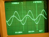
You will see in the picture (compared to the AC analyses) that the HF roll-off is at 570KHz instead of 455KHz simulated. There is off-course a large tolerance on those ceramic feedback capacitors and also a readout error. However I find the difference just a little too big to be just that?
At 15MHz is the simulated unity gain frequency. In reality it is around 10MHz. This means the roll-off slope is steeper than simulated. The top corner is more to the right in frequency and the bottom point more to the left. I would think there is an extra pole somewhere that creates the faster roll-off. But again it could just be tolerance, however why the opposing action than?
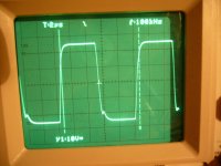
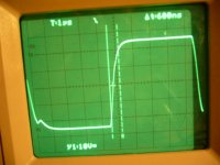
The slewrate is OK. 66V/uS from 10% to 90% signal on 100KHz Square Wave.
The phase story also seems a bit bad. On the picture you see a 80° phase lag between input and output at 570KHz. According to the simulation it is 52°. Why would that be? This is at 570KHz. It looks even worse when one thinks that simulation shows a 47° phase at the exact HF roll off point whereas in reality it is 80° at that point (freq is not the same since HFRO point is different). Any clues?
I don't have a picture but the phase story quickly deteriorates in reality. At 1MHz the gain is 26 whereas in the simulation it is 23,5. Probably because the HFRO point is higher than the one on the simulator. The Phase here is allready 108° (PCB) and 67° (simulation). At 10MHz (maximum of function generator) the gain in reality is 0dB (approx) and 3,8dB in the simulator. The pase in reality is very very near to 180° ... maybe 175° ... simulated = 113° ... What's wrong?
Remember there is no input HF shunt capacitor yet. You might have noticed on the square wave that the lower side shows strange signs? I don't know what it is. I see it is MUCH less on the top side. But it is also there (maybe 10x less). When I insert such a cap of 1000pF this is gone for 99%. However slewrate drops from 66 to 55V/us. Maybe this behavior without cap is what you and Bob told me. The charging of the input diff Q caps?
I also send the .CIR in this post.
Thnx
Olivier
FIRST OF ALL - HAPPY NEWYEAR TO EVERYONE HERE ON DIY !!!! MAY 2011 BRING ALL OF THE BEST FOR YOU AND YOUR LOVED ONES
Hi Edmond, (mijn beste wensen voor 2011!)
You are right about changing one thing at a time. But while waiting for your analyses I try to go forward too and in the heat of testing some components have changed. Hereby you will find the schematic as is set up on the PCB. The only thing that is different is the Vbias circuit which is on te PCB but not in the schematic. I believe this to be of no influence.
The dummy OPS is disconnected for the moment but can be reconnected any time. I noticed however, it's adding didn't change much if not nothing.
The RC network between IPS out and VAS in seems to be useful (R/C 500/501). However, removing it doesn't make the amp go into RF bursts anymore since I raised the degenaration resistors from 20R to 182R.
The HF Roll-Off circuit for the CMCL on the other side remains a mistery. Removing it makes everything OK. Adding it (and any resistor 33R or 100R) creates instability. I wonder why?
I lowered the 1K resistors R102/R103 to 475R. On the simulator it shows better PM & GM but it raises the VAS Iq from 7mA to 13mA which is a bit high. However still within the SOAR of the Q's. They are Heatsinked Anyway. Running at 50V the power is acceptable. Later moving up to 75V rails this will need to be adressed. But that's later.
Another thing that I dislike is the fact that it disbehaves when inserting a Zener or LM4040 Vref into the Darlington Leg of the VAS (to meet the Vref of the Qcc base in order to avoid saturating the Qcc). When added, there is quite some overshoot on the signal. However I wouldn't call it simply overshoot. It's more like peaking up following the rise curve and then chopped vertically down towards the final output voltage (top of the square voltage). So it's not a typical overshoot phenomena, I think at least (too bad I don't have a picture).
You will see in the picture (compared to the AC analyses) that the HF roll-off is at 570KHz instead of 455KHz simulated. There is off-course a large tolerance on those ceramic feedback capacitors and also a readout error. However I find the difference just a little too big to be just that?
At 15MHz is the simulated unity gain frequency. In reality it is around 10MHz. This means the roll-off slope is steeper than simulated. The top corner is more to the right in frequency and the bottom point more to the left. I would think there is an extra pole somewhere that creates the faster roll-off. But again it could just be tolerance, however why the opposing action than?
The slewrate is OK. 66V/uS from 10% to 90% signal on 100KHz Square Wave.
The phase story also seems a bit bad. On the picture you see a 80° phase lag between input and output at 570KHz. According to the simulation it is 52°. Why would that be? This is at 570KHz. It looks even worse when one thinks that simulation shows a 47° phase at the exact HF roll off point whereas in reality it is 80° at that point (freq is not the same since HFRO point is different). Any clues?
I don't have a picture but the phase story quickly deteriorates in reality. At 1MHz the gain is 26 whereas in the simulation it is 23,5. Probably because the HFRO point is higher than the one on the simulator. The Phase here is allready 108° (PCB) and 67° (simulation). At 10MHz (maximum of function generator) the gain in reality is 0dB (approx) and 3,8dB in the simulator. The pase in reality is very very near to 180° ... maybe 175° ... simulated = 113° ... What's wrong?
Remember there is no input HF shunt capacitor yet. You might have noticed on the square wave that the lower side shows strange signs? I don't know what it is. I see it is MUCH less on the top side. But it is also there (maybe 10x less). When I insert such a cap of 1000pF this is gone for 99%. However slewrate drops from 66 to 55V/us. Maybe this behavior without cap is what you and Bob told me. The charging of the input diff Q caps?
I also send the .CIR in this post.
Thnx
Olivier
Oops
I forgot the attachement in the revious post ... here they are
(why do we always need to remember this just after clicking submit? )
)
I forgot the attachement in the revious post ... here they are
(why do we always need to remember this just after clicking submit?
)Attachments
-
 100KHZ_SQUARE.JPG95.4 KB · Views: 313
 -
 570KHZ_SINE.JPG98 KB · Views: 299
 -
CMCL_20_TMC&TPC_AsBuilt7.cir.txt92.8 KB · Views: 67
-
CMCL_20_TMC&TPC_AsBuilt7_Voltages.pdf22.6 KB · Views: 61
-
CMCL_20_TMC&TPC_AsBuilt7_Currents.pdf25.7 KB · Views: 63
-
CMCL_20_TMC&TPC_AsBuilt7_AC_Analyses.pdf62.1 KB · Views: 75
-
 SLEWRATE.JPG91.1 KB · Views: 296
AC analyses 2
Hi there,
Today I went on doing some testing. I added some rel measured points to the bodeplot I sent yesterday. I also noticed an error in my description yesterday. The phase response is worse. I wrote that by 10MHz the phase delay reached a 180°. Well, stangly it reaches nearly 360° !!!
The 180° point is rather around 3MHz. I have drawn the overshoot of 180° back upwards in the graph (this is not a sudden phase shift ! )
My questions are still the same ...
Thnx
Olivier
Attachments
AC-3
I plotted another measurement on the AC graph / Bodeplot.
In pink is the response between output and input
In bright green is the response between feeback input and input of the IPS.
I watched more carefulle what happens when it crosses the 180° margin. At that point the output signal is completely ZERO. Then it becomes bigger again but inverted to what it was before it reached 180°.
Thats logical
This happens around 8MHz... at 10MHZ the feeback ouput reaches a 50mVpp value wich since 8MHz is growing but my generator is limited to 10MHz ... I wonder till where it would grow??
Is this anything interesting for analyses?
Olivier
Attachments
NFB loop reponse.
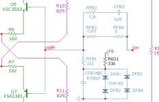
Hi Olivier,
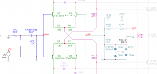
You get more reliable results for the NFB loop gain, when you put the test signal at the FB network and (of course) connect the non-inverting input to ground. Remember to restore the DC operating point by adding a resistor (R610) between the output (=FB) and the electrolytic cap. See pic. below.
Now, just observe or plot the relationship between V(Fb) and V(Vin). That's the NFB loop gain and loop phase. The phase margin is direct readable at V(FB)/V(Vin)=0dB
Cheers,
E.
PS: Forget the open loop response. It's not interesting.
The only loops that really matter (with regard to stability) are real loops:
1. Negative feedback loop (or global NFB loop, or major loop)
2. Miller loop (or minor loop)
3. Common mode control loop (CMCL).
The so called 'open loop' is no loop at all.
Hi Olivier,
You get more reliable results for the NFB loop gain, when you put the test signal at the FB network and (of course) connect the non-inverting input to ground. Remember to restore the DC operating point by adding a resistor (R610) between the output (=FB) and the electrolytic cap. See pic. below.
Now, just observe or plot the relationship between V(Fb) and V(Vin). That's the NFB loop gain and loop phase. The phase margin is direct readable at V(FB)/V(Vin)=0dB
Cheers,
E.
PS: Forget the open loop response. It's not interesting.
The only loops that really matter (with regard to stability) are real loops:
1. Negative feedback loop (or global NFB loop, or major loop)
2. Miller loop (or minor loop)
3. Common mode control loop (CMCL).
The so called 'open loop' is no loop at all.
Attachments
LOOP AC Analyses
Hi Edmond,
I tested the circuit with the modification you proposed. I attached the pdf of the AC analyses in this post. For now I only simulated it.
The 0dB GAIN frequency is at 445KHz. That is exactly where the previous AC analyses had its -3dB point but that is logical.
The phase margin here (445KHz) is about 105°. Compared to the previous AC analyses this was 135°. So now it looks a bit worse than before ...
In reality (on the PCB yesterday) I placed the inputsignal at the bases of the diff amp Q's (left side) and the scope probe at the VAS output. This showed a result at 445KHz of 120° PM which is precisely in between 105 and 135 ...
However, it could be I have to compare -3dB point Frequencies... In reality the -3dB point was at 650KHz instead of 455KHz (don't know why) ... at that frequency the phase lag was 75° or a PM of 105° which in turn is EXACTLY equal to the simulation of today ...
But I extrapolate my knowledge into wishfull thinking maybe ... First of all is the measurement comparable to the simulation as I did before or is it compareable to what you wanted me to simulate ??? Second, is my assumption to compare PM between reality and sim at 2 diffrent freq realistic (knowing off-course they both represent the -3db point ... once in sim and once in reality ....)
Let me know...
Thnx
Olivier
Attachments
bubble
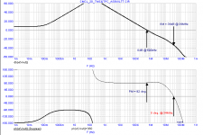
Hi Olivier,
You better avoid the phase bubble at 4MHz, caused by a too large CFB2. It has negative impact on the gain margin (18dB @ 65MHz), Besides, you don't need a phase margin of 120° or so. 90° is enough. Also, a cap of 10pF might provoke more HF ingress.
With CFB2 = 1.8pF and RFB2 = 12k, you will get a cleaner response and a much better gain margin: 34dB.
Cheers,
E.
Attachments
Test
Hi Edmond,
The smallest cap I have is 5.6pF ...
I will do the simulation with 5.6p and also the real measurement to see what happens and what the differences are.
I will iterate this test, removing the 5.6pF cap altogether. So I can see the impact of it in simulation & in reality compared to the presence of a 5.6pF cap.
For now my major problems are :
1) Gain / Phase response seems different from simulated quite much. (therefore i will do the testing as described above).
2) The CMCL rolloff circuit R/C 500/501 must be removed because it causes RF bursts easily
3) The zener Vref or an LM4040 Vref in the darlington leg of the VAS (used as clamp) is removed and shorted because it causes RF bursts
There are other problems but of an inferior order I believe so lets concentrate on these ones. Maybe one solution solves everything ...
If you have any idea of what it could don't hesitate i would say...
Schol,
Olivier
Test
Hi Edmond,
I tested today without CFB2 as I don't have such small caps.
Here is the result of the simulated AC analyses with added asterisks representing the real measurements.
As you can see, phase dips down way too soon.
Another thing is that at higher frequency (>500KHz) the output signal is all noisy. Rather then noisy it shakes up an down very fast. At 2MHz I could not measure the gain ratio since the bouncing is too much.
Yet another thing I want to say is that when I bring up the input voltage (to compensate for falling gain -> to maintain a good reading on the scope because of the bouncing) the signal gets much worse (bouncing) when the generator reaches exactly 2,00Vpp. At that point the generator makes a click like a relay sound (probably to step up the range)... is this of any concern?
Hope you can use the testresults ...
Cheers,
Olivier
Attachments
Hi Olivier,
The ULGF of the real amp is 20% higher. A bit too much to be attributed to only component tolerances. Regarding more phase lag, how large is capacitance of the probe connected to the output? If it is too high, this could explain the difference with the sim. In that case I would reinstall the dummy OPS.
Cheers,
E.
OK
Hi Edmond,
I don't know what the cap value of the probe is. I will check it out this evening and anyway reconnect the dummy OPS for comparison.
What do you think is a good frequency for a high-end amp to a)have it's high closed loop roll-off point and b)its unity gain frequency (this is related of course if it's a -20dB slope ...) ?
Some say a) 200Khz b) around 4Mhz
Others and Bob describes in his book a) 500 to 2000 Khz and b) not specified but must be around 20 to 50 Mhz ...
As I am using a 4L PCB it is built like this :
TOPLAYER : tracks + full island pours connected to a terminal
MIDLAYER1 : almost full copper common ground (dirty ground) connected to 1 terminal
MIDLAYERS2 : some tracks mostly signal ground + island pour connected to 1 terminal
BOTTOMLAYER: same description as TOPLAYER....
So there are 3 terminals : TOPSHIELD, MIDLAYER2SHIELD, BOTTOMSHIELD
And 1 terminal : COMMONGROUND
these are 4 seperate terminnals.
(there are off course others for SIG GND, VCC, VEE, INPUTSIG,....)
I like those planes, and shields thinking of RF pickup, EMI , .... But they probably must introduce lots of capacitance between tracks & layers ...
If one would not look for the money ... is this rather a GO or a NOGO method?
Going for lunch now ...
Olivier
- Status
- This old topic is closed. If you want to reopen this topic, contact a moderator using the "Report Post" button.
- Home
- Amplifiers
- Solid State
- HEEEELLLPPP : M. Randy Slone Mirror Image Topology Construction - Troubles