hi Kenpeter, I made a Kuroda-Tanaka amp on simulation here.
http://www.diyaudio.com/forums/solid-state/165007-ltspiceiv-librairies-management.html#post2152058
The amp is buried into this post because I found difficult, under LTspiceIV, to add BJT devices in the librairy. I wanted this issue to be solved before publishing the simulation file. I didn't want to uncumber this present thread (the non-switching concepts) with librairy management questions.
So, now you can see how Tanaka (Sansui) non-switching bias is working.
According to the simulation, the bias current needs to be high for keeping the non-switching feature at high power levels.
Kenpeter, I think that your approach using one cold Schottky diode as sensor behaves better on simulation. It provides more control.
Regards,
Steph
Here two additional links of such amplifiers:
1) Low-distortion Super-pair Buffer
http://www.diyaudio.com/forums/soli...-super-pair-buffer-simulation-schematics.html
2) Class-B without crossover-distortion
http://www.diyaudio.com/forums/solid-state/160285-class-b-w-o-crossover-distortion-1975-a.html
1) Low-distortion Super-pair Buffer
http://www.diyaudio.com/forums/soli...-super-pair-buffer-simulation-schematics.html
2) Class-B without crossover-distortion
http://www.diyaudio.com/forums/solid-state/160285-class-b-w-o-crossover-distortion-1975-a.html
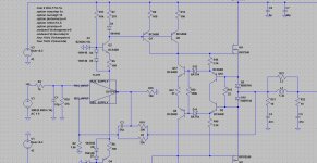
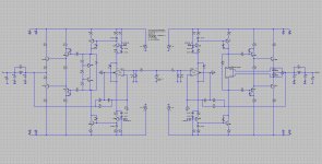
hi Kenpeter, attached you will find a revision now taking advantage of the guaranteed Thornton current, with R15 = 22 ohm.
This circuit contains genetic from :
- Kuroda for the overall simplicity thanks to an opamp as front-end, current feedback topology (high current in the VAS if required), and MOSFET output. Later on, I'll simulate lateral MOSFETs instead of the vertical MOSFETs we have here as there may be a problem with lateral MOSFETs with their Vgs of approx 0.8V each, maybe not enough for powering the Iq servo-loop circuitry.
- Dodson for measuring the output current using diodes, driving two transistors in series in a feedback loop, acting as a variable Vbe multiplier, a scheme that's not far away from Tanaka's scheme presented after Dodson.
- Thornton for guaranteeing a minimal current in the MOSFETs, using fast schottky diodes and current sources coming from the supply rails. In Thornton's arrangement, in case of a big positive voltage at the output, with the high-side MOS massively conducting, the low-side MOS is forced to conduct also because the current source connected to the positive rail had the capability to manipulate the low-side MOS source electrode, disconnected from the load because of the Schottky, making the low-side MOS source electrode more positive, hence building up a Vgs voltage forcing the low-side MOS to eat this current. One can thus see the low-side MOS being common-gate driven, for eating the constant current tending to make his source electrode more positive than his gate electrode.
- Kenpeter for degenerating and simplifying the said current sources, replacing them by a single alternating dual-purpose current source connected to fugitive +0.5 / -0.5 rails surrounding the output signal. Is this analysis valid ? R15 seems to have a very limited capability to manipulate the MOS source voltages, like said above. I need time to think about this.
- Cnockaert for allowing a small quiescent current, by compensating all the junctions. The two measuring Schottky get compensated by the two Schottky in the feedback loop. The two junctions in the series Vbe bias multiplier get compensated by the emitter followers junctions. First-order thermal sensitivity is zeroed. The operating current is thus defined by resistor ratios and diode current density ratios. Bulletproof and integrable inside ICs.
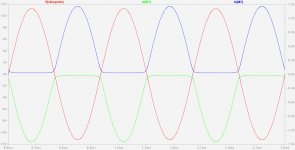
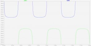
This circuit, as such, defines a quiescent current in the MOS equal to 75mA. When this circuit is delivering power, it uses 50mA of the quiescent current for softening the crossover (yes indeed, that's a genuine Class AB Soft-Switching), and 25mA as guaranteed Thornton current. When the current gets 100% driven, like outputting 3 or 4 amp, zooming on the waveforms, one can see that the 50mA "soft cushion" is still in place, softening the transitions, applied to a flat baseline of 25 mA Thornton guaranteed current.
If you look closely to the circuit, you will see a small wiring simplification compared to the previous one. The emitter followers Q2 and Q18 in the bias servo circuitry have now their collectors connected in series, instead of independently taking their supplies from the gate drive lines. If you walk LTspiceIV current probe and sample the current flowing from Q18 collector to Q2 collector, you are not going to like the waveform shape. It is highly non-sinusoïdal. But the circuit is working properly, and generates less distorsion than the Kuroda reference amp, on the right side (see the .fourier report). Clearly, I prefear the emitter followers current waveforms of previous version (with independent collector supplies taken from the gate drive), but on the other hand, I like the clean aesthetics of the new schematic.
See attached .zip - it contains everything.
Steph
This circuit contains genetic from :
- Kuroda for the overall simplicity thanks to an opamp as front-end, current feedback topology (high current in the VAS if required), and MOSFET output. Later on, I'll simulate lateral MOSFETs instead of the vertical MOSFETs we have here as there may be a problem with lateral MOSFETs with their Vgs of approx 0.8V each, maybe not enough for powering the Iq servo-loop circuitry.
- Dodson for measuring the output current using diodes, driving two transistors in series in a feedback loop, acting as a variable Vbe multiplier, a scheme that's not far away from Tanaka's scheme presented after Dodson.
- Thornton for guaranteeing a minimal current in the MOSFETs, using fast schottky diodes and current sources coming from the supply rails. In Thornton's arrangement, in case of a big positive voltage at the output, with the high-side MOS massively conducting, the low-side MOS is forced to conduct also because the current source connected to the positive rail had the capability to manipulate the low-side MOS source electrode, disconnected from the load because of the Schottky, making the low-side MOS source electrode more positive, hence building up a Vgs voltage forcing the low-side MOS to eat this current. One can thus see the low-side MOS being common-gate driven, for eating the constant current tending to make his source electrode more positive than his gate electrode.
- Kenpeter for degenerating and simplifying the said current sources, replacing them by a single alternating dual-purpose current source connected to fugitive +0.5 / -0.5 rails surrounding the output signal. Is this analysis valid ? R15 seems to have a very limited capability to manipulate the MOS source voltages, like said above. I need time to think about this.
- Cnockaert for allowing a small quiescent current, by compensating all the junctions. The two measuring Schottky get compensated by the two Schottky in the feedback loop. The two junctions in the series Vbe bias multiplier get compensated by the emitter followers junctions. First-order thermal sensitivity is zeroed. The operating current is thus defined by resistor ratios and diode current density ratios. Bulletproof and integrable inside ICs.
This circuit, as such, defines a quiescent current in the MOS equal to 75mA. When this circuit is delivering power, it uses 50mA of the quiescent current for softening the crossover (yes indeed, that's a genuine Class AB Soft-Switching), and 25mA as guaranteed Thornton current. When the current gets 100% driven, like outputting 3 or 4 amp, zooming on the waveforms, one can see that the 50mA "soft cushion" is still in place, softening the transitions, applied to a flat baseline of 25 mA Thornton guaranteed current.
If you look closely to the circuit, you will see a small wiring simplification compared to the previous one. The emitter followers Q2 and Q18 in the bias servo circuitry have now their collectors connected in series, instead of independently taking their supplies from the gate drive lines. If you walk LTspiceIV current probe and sample the current flowing from Q18 collector to Q2 collector, you are not going to like the waveform shape. It is highly non-sinusoïdal. But the circuit is working properly, and generates less distorsion than the Kuroda reference amp, on the right side (see the .fourier report). Clearly, I prefear the emitter followers current waveforms of previous version (with independent collector supplies taken from the gate drive), but on the other hand, I like the clean aesthetics of the new schematic.
See attached .zip - it contains everything.
Steph
Attachments
-
 Kuroda Dodson Thornton Kenpeter Cnockaert 75mA bias TL071 60W FET amp - schematic.jpg237.6 KB · Views: 1,511
 -
 Kuroda Dodson Thornton Kenpeter Cnockaert 75mA bias TL071 60W FET amp - 22Vpp 8 ohm load.jpg138.7 KB · Views: 1,453
 -
 Kuroda Dodson Thornton Kenpeter Cnockaert 75mA bias TL071 60W FET amp - 22Vpp 8 ohm load (zoom).jpg77 KB · Views: 1,279
 -
Kuroda Dodson Thornton Kenpeter Cnockaert 75mA bias TL071 60W FET amp.zip328.9 KB · Views: 254
Can somebody advise how to test the temperature dependencies of the circuit described above, using LTspiceIV ?
I'm not talking about the MOSFETs parameters. I'm talking about the four Schottky and the four BJTs involved in the bias servo circuitry.
1. Is it possible to define a global temperature and make a sweep on this value, for graphically obtaining the quiescent current in function of the global temperature ?
2. Is it possible to define warm and cold zones, and see how the temperature dependency evolves ? Something like having the two big Schottky temperature 25°C above the rest of the circuit.
Thanks,
Steph
I have no idea how you would simulate it? But the solution I would
suggest is bolt a heat wasting device to the same sink as the diode
stack, and warm the crossing to taste with some sorta servo loop.
I don't know how you might effectively monitor the current minimum?
Maybe just barely keep an LED (optocoupler) from going out???
Or if you warm comparator transistors, drive crossing bias down.
Could just bolt these to the output sink, but chances you'd just
spiral totally into hard B without significantly lowering the output
temperature. But it would probably stop a diode stack runaway
into class A or worse... If the only concern was one of safety...
Neither idea is really even quarter baked...
Last edited:
Q18 + Q2 are wired Collector to Collector. Was that your intent?
Wouldn't the higher HFE drag the midpoint voltage all the way into
itself, putting it into a deep saturation? Maybe the sim is too well
matched to show that? Maybe if only one or the other saturates
and stays stuck that way isn't a problem anyhow???
I would just use Q2 by itself. And ditch Q18, D11, D12. Not much
different than the fully saturated collector latchup situation as
described above, and saves 3 parts. OK R48 R50 too, maybe it
saves five parts...
Last edited:
by post #32 about
http://www.diyaudio.com/forums/soli...8-2sk60-2sj26-2sk76-2sk180-4.html#post2152954
there are informations about various patents concerning SIT's - perhaps also of interest here
http://www.diyaudio.com/forums/soli...8-2sk60-2sj26-2sk76-2sk180-4.html#post2152954
there are informations about various patents concerning SIT's - perhaps also of interest here
Hi kenpeter, I did it on purpose for getting a more aesthetical schematic, as explained in the presentation. I knew this was going to degrade the servo-loop, but to my surprise, the servo-loop still works intact. Amazing. Robust stuff. So, why not ? Must say you are right in saying that LTspiceIV is an idealized view on the penomenon. We need to remain cautious. I'm quite satisfied and comfortable with the latest release because all junctions get compensated one by one, Schottky by Schottky and BJT by BJT. You may not like the amount of transistors involved (four of them), but compensating the junctions one by one is a must for not needing to overcompensate the thermal behaviour, and returning back to a dumb class-B when warming up. On the other hand I'm appreciating simplicity, so if you could post a sketch of the simplification you describe, it would be a great help, much appreciated.Q18 + Q2 are wired Collector to Collector. Was that your intent ? I would just use Q2 by itself. And ditch Q18, D11, D12.
I'll take some time, later on, for assessing the thermal behaviours of various implementations, using LTspiceIV.
At this stage, I don't know how to warm up the whole circuit using LTspiceIV, and I don't know how to selectively warm-up some sections or components of the circuit. Any help much appreciated.
Cheers,
Steph
Well, whats confusing to me is that Bob makes it sound so much worse
for the common source configuration. Yet Qg + Qdg sum up the same
either way you go. If I can charge and discharge those Coulombs in the
required timeframe, does the apparent capacitance change matter?
The drive circuit can source or sink 5.5mA into the gate(s), and that
seemed plenty fast enough on the simulation for the output voltages
and currents and bandwidth we were trying to achieve.
I just want to know if his warning refers to something the simulation
is not telling us? I don't take anything Bob sais lightly. Aim to be the
next Bob Cordell after he's dead. But untill then, Long Live the King!!!
If he sais this is not going to work, I want to fully understand why?
The amplifiers I final test every day are Class-D EVMs, and designed
by someone else. I'm not even in the loop on the design side. My real
world hands-on experiences may not be relevant to what I actually
need to know to design a flawless class AB amplifier. I am not above
making clueless mistakes.
Hi Kenpeter,
There are a lot of things about the behavior of power MOSFETs that are not well-understood, including pitfalls in simulation and lack of adequate linear-region characterization in spec sheets. Part of this is a result of the situation that the biggest usage of power MOSFETs is in switching applications, like switching power supplies and class D amplifiers.
This DOES NOT mean that vertical power MOSFETs are not great devices for class AB audio amplifiers, as some have foolishly claimed.
On spec sheets, the gate charge diagram usually supplied for power MOSFETs can be extremely confusing to even astute engineers. One has to look carefully at how it is tested to properly understand it, especially the flat region where Miller effect is dominating. This presentation has misled many people into believing wrongly that gate-source capacitance suddenly increases when the device turnes on. Gate-source capacitance in fact is relatively flat with Id. The biggest cause of change in input capacitance Ciss is the gate-drain component of which I was speaking in the earlier post.
The dramatic in crease in Cgd is so stunning that I did indeed measure it for myself, just to prove that it was not something that was a misleading artifact of the switching measurement mindset of the guys that make the spec sheets. It is indeed real. This is a potentially serious issue for MOSFET amplifiers when they are at high output levels near clipping when Vdg becomes small.
To make matters worse, the SPICE models for Cgd are cr@p. Most of them work only semi-reasonably in a switching context. The LTspice VDMOS model is an exception. In my experience it seems to give reasonable results.
Most SPICE models do a terrible job of modeling Id vs Vgs and gm vs Ic at low current. This is because they assume that the MOSFET is a square law device across the board. It is not. The missing piece is called sub-threshold conduction, or weak inversion. The square law model has Id go to zero at the threshold voltage. In fact, the behavior transitions to exponential behavior at low current (like that of a BJT). Just like a BJT, a MOSFET at low Id has an Id vs Vgs slope analogous to the 60 mV/decade slope of a BJT. Except that the analogous slope for a power MOSFET is more like 500 mV/decade, corresponding to lower transconductance for a given operating current.
The transition region from square law behavior to exponential behavior often lies in the range where we typically bias MOSFETs, around 150 mA. Simulations of class AB crossover distortion are largely worthless as a result.
The EKV model does accurately model the vertical power MOSFET in both regions, but there are virtually no publicly-available EKV models for power MOSFETs. LTspice does support the EKV model in their standard SPICE model, but unfortuantely does not support the EKV model in connection with their VDMOS model. So you cannot get both accurate DC and capacitance modelling at the same time in a straightforward way.
Cheers,
Bob
So, what do I do? I can easily raise reserve current above the low end mess.
But the high end mess seems to require an unmodelable drive current???
If I simulate with a worst case (1500pf?) capacitance in parallel with Cgd?
Would that be a valid simulation to determine if I have an adequate drive
to operate when the drain swings lower than the gate?
But the high end mess seems to require an unmodelable drive current???
If I simulate with a worst case (1500pf?) capacitance in parallel with Cgd?
Would that be a valid simulation to determine if I have an adequate drive
to operate when the drain swings lower than the gate?
...I thought the purpose of a patent was to attempt to describe a highly precise process/product/idea in such vague terms that any implementation that looks even slightly similar could be argued over by patent lawyers - hence keeping their kind in business ")
And to (vaguely) answer the original question of whether or not you would be breaching copyright - I believe any embodyment of the patented idea that is produced and distributed in order to make profit would be a breach of copyright.
You'll have to be pretty sure exactly what each patent covers, then be sure you are not in breach before sharing any such implementation.
In addition, even if you are not making a profit on any such design, you may be considered as causing damage to the copyright holder if any action you perform causes them to lose potential income - this may be fuel enough for a lawsuit.
In practical terms, making a few samples of a circuit and giving it to your friends is far too small an impact for the original manufacturer to risk a PR nightmare over.
Last edited:
I got chewed out yesterday for spending too much work time running simulations
rather than testing amplifiers. I can do both at the same time, but what can you
do about perceptions of those who think it can only be one way or the other???
Anyways, forgive no time to attach drawings, but I did run some last night at
home. It seems that bumping drive quiescent currents up 40mA (including the
crossing error comparator) is sufficient to drive a 96KHz waveform that looks
reasonably sinusoidal within 2V of either rail. Even with 1500pF sandbagging
each drain to gate. And works fine/stable with 1500pF removed too.
This requires bigger transistors 2905 and 3019 where drive currents got bigger.
And I added a 330R base to base in both input and output Allisons. This gives
another standing 4mA reserve current bleed on all the drive transistors. Extra
insurance they don't turn off... Straight up and down 330R, not cross coupled...
The cross couple resistors drop to 33R, consistant with new 44mA quiescent.
And the main bleed across the output diodes, drop to 4.7R
The last Issue I'm fighting, and this may have been a problem even before
the current increase. The soft current limiter wants to ring into 2ohm loads
and less. It does not ring so bad as to violate SOA, but its an annoyance...
Its not intended to drive less than 8ohm load without soft clipping anyway,
but this ringing misbehavior is an embarrassment that should be fixable.
You have to challenge the sim with 22K or higher to see the ringing, won't
show up any problem in the 1KHz simulation.
Last edited:
hello,
here you can find some simulations on LTspiceIV, comparing two different Class AB Non-Switching arrangements. They both sample the voltage using emitter Schottky diodes instead of using emitter resistors.
This dramatically reduces the dynamic and the saturation issues of the servo-loop managing the bias. Thanks Kenpeter for bringing this idea forefront.
From a .FOUR 1kHz on a .TRAN simulation of 150 ms, only taking the last 100 ms for measuring a fully settled system, we get :
THD with 100mV 1kHz at the input of the amplifier :
0.000024 % for the normal Vbe multiplier (no decoupling cap) :
0.000698% for Soft Non-Switching 001
0.000087% for Soft Non-Switching 002
THD with 100mV 1kHz at the input of the amplifier :
0.000199 % for the normal Vbe multiplier (no decoupling cap) :
0.000237% for Soft Non-Switching 001
0.000187% for Soft Non-Switching 002
Version 001 approach is not satisfactory :
1. The bias feedback loop based on two differential amplifiers is highly complex. Open the SNS_controller_001 subcircuit, and you'll see for yourself.
2. For this particular application, it was decided NOT to rely on an external power supply, and this explains the extra complexity involving proper current sources still working on a +1.65V / -1.65V supply like available when a BJT darlington output stage is used.
3. Due to the minimal supply requirements, version 001 is not compatible with lateral MOSFETs having a threshold of 0.8V, and is not compatible with CFP having only one Vbe voltage drop.
4. The loop gain and the range of the two bias-servo differential amplifiers are fixed. The loop gain and the range need to be high for quickly and fully boosting the polarization of the non-conductig output device, for bringing it into weak conduction when the other output device is delivering a high current. This is how the Non-Switching feature is implemented.
5. But there is a flip side. The servo-loop reacts abruptely when entering the crossing region, a delicate area where the dI/dt slopes are high, with the instantaneous currents temporary vanishing to nearly nothing (actually, the quiescent current). We can see the servo-loop generating a nasty crossover glitch, and sometimes, oscillation bursts containing 2 or 5 damped cycles at several MHz.
6. Such glitch can be seen by measuring the differential voltage across the two inputs of the TL071. Under Waveform Wiewer, click the voltage probe for getting the red probe, maintain it clicked, move the cursor, and you'll get the black voltage probe. This is how to graph differential voltages using LTspiceIV. The bigger the input signal, the bigger the glitch.
IMO, the flaw of version 001 lies in the "beautiful, symmetric" twin differential amp structure. Using this approach we introduce not one, but two loop gains, that can't be identical both in strenght and speed due to the non perfect NPN-PNP symmetry. That's not relevant when you think about managing high currents, with one servo-branch being nearly saturated hence inactive (the one that's associated to the conducting device), and the other servo-branch, the active one, acting for restoring some conduction into the the other output device, the one that would get out of conduction. BUT ... what about during crossing, when both device currents tends to equal the programmed quiescent current ? Answer : both servo-loop branches get then active. They both operate outside of saturation, with their full gain and their own speed. And speed is of importance, because it is during crossing that the dI/dt figure is the highest. So you see the problem : two unmatched functional blocks, having different gains and speed, one just exiting saturation, and the other one still alive -> they tend to fight each other -> you then get the crossover glitch !
Must say that when sketching the SNS_controller_001 subcircuit, I had the impression that I was reinventing the wheel, like coming close to the LT1166 approach.
But having now figured out why version 001 delivers a glitch, I'm now nearly sure that the LT1166 is not relying on two differential amplifiers inside.
If somebody could tell me what is the actual structure of the LT1166, I'll make a dedicated simulation. I'm now sure that the LT1166 is better than what I've done in version 001. The LT1166 can cope with the high dynamic of a emitter resistor used as current sensor, so surely the LT1166 will behave more than adequate when using a Schottky as current sensor. Or maybe not ?
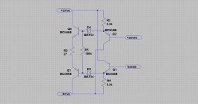
Version 002 approach is a viable alternative to the classic Vbe multiplier.
See the SNS_controller_002 in attached .jpg.
Compared to a conventional Vbe multiplier, version 002 exhibits a very slight THD degradation at low amplitudes. It gets better at big amplitudes, where version 002 has the best THD, slightly better than a conventional Vbe multiplier. It is amazing to see such a straightforward circuit performing so nicely. Note how the collectors of the emitter followers are connected, in series. In theory, they should go independently the the other rails (+drive / -drive), but I liked the idea of having them in series, it is graphically more appealing.
Version 2 approach doesn't generate a spike at crossover.
Version 2 looks promising.
Anyway, the figures and graphs are what LTspiceIV says, with the transistor models I have used. Don't know how this connects with real world results ...
Cheers,
Steph
here you can find some simulations on LTspiceIV, comparing two different Class AB Non-Switching arrangements. They both sample the voltage using emitter Schottky diodes instead of using emitter resistors.
This dramatically reduces the dynamic and the saturation issues of the servo-loop managing the bias. Thanks Kenpeter for bringing this idea forefront.
From a .FOUR 1kHz on a .TRAN simulation of 150 ms, only taking the last 100 ms for measuring a fully settled system, we get :
THD with 100mV 1kHz at the input of the amplifier :
0.000024 % for the normal Vbe multiplier (no decoupling cap) :
0.000698% for Soft Non-Switching 001
0.000087% for Soft Non-Switching 002
THD with 100mV 1kHz at the input of the amplifier :
0.000199 % for the normal Vbe multiplier (no decoupling cap) :
0.000237% for Soft Non-Switching 001
0.000187% for Soft Non-Switching 002
Version 001 approach is not satisfactory :
1. The bias feedback loop based on two differential amplifiers is highly complex. Open the SNS_controller_001 subcircuit, and you'll see for yourself.
2. For this particular application, it was decided NOT to rely on an external power supply, and this explains the extra complexity involving proper current sources still working on a +1.65V / -1.65V supply like available when a BJT darlington output stage is used.
3. Due to the minimal supply requirements, version 001 is not compatible with lateral MOSFETs having a threshold of 0.8V, and is not compatible with CFP having only one Vbe voltage drop.
4. The loop gain and the range of the two bias-servo differential amplifiers are fixed. The loop gain and the range need to be high for quickly and fully boosting the polarization of the non-conductig output device, for bringing it into weak conduction when the other output device is delivering a high current. This is how the Non-Switching feature is implemented.
5. But there is a flip side. The servo-loop reacts abruptely when entering the crossing region, a delicate area where the dI/dt slopes are high, with the instantaneous currents temporary vanishing to nearly nothing (actually, the quiescent current). We can see the servo-loop generating a nasty crossover glitch, and sometimes, oscillation bursts containing 2 or 5 damped cycles at several MHz.
6. Such glitch can be seen by measuring the differential voltage across the two inputs of the TL071. Under Waveform Wiewer, click the voltage probe for getting the red probe, maintain it clicked, move the cursor, and you'll get the black voltage probe. This is how to graph differential voltages using LTspiceIV. The bigger the input signal, the bigger the glitch.
IMO, the flaw of version 001 lies in the "beautiful, symmetric" twin differential amp structure. Using this approach we introduce not one, but two loop gains, that can't be identical both in strenght and speed due to the non perfect NPN-PNP symmetry. That's not relevant when you think about managing high currents, with one servo-branch being nearly saturated hence inactive (the one that's associated to the conducting device), and the other servo-branch, the active one, acting for restoring some conduction into the the other output device, the one that would get out of conduction. BUT ... what about during crossing, when both device currents tends to equal the programmed quiescent current ? Answer : both servo-loop branches get then active. They both operate outside of saturation, with their full gain and their own speed. And speed is of importance, because it is during crossing that the dI/dt figure is the highest. So you see the problem : two unmatched functional blocks, having different gains and speed, one just exiting saturation, and the other one still alive -> they tend to fight each other -> you then get the crossover glitch !
Must say that when sketching the SNS_controller_001 subcircuit, I had the impression that I was reinventing the wheel, like coming close to the LT1166 approach.
But having now figured out why version 001 delivers a glitch, I'm now nearly sure that the LT1166 is not relying on two differential amplifiers inside.
If somebody could tell me what is the actual structure of the LT1166, I'll make a dedicated simulation. I'm now sure that the LT1166 is better than what I've done in version 001. The LT1166 can cope with the high dynamic of a emitter resistor used as current sensor, so surely the LT1166 will behave more than adequate when using a Schottky as current sensor. Or maybe not ?
Version 002 approach is a viable alternative to the classic Vbe multiplier.
See the SNS_controller_002 in attached .jpg.
Compared to a conventional Vbe multiplier, version 002 exhibits a very slight THD degradation at low amplitudes. It gets better at big amplitudes, where version 002 has the best THD, slightly better than a conventional Vbe multiplier. It is amazing to see such a straightforward circuit performing so nicely. Note how the collectors of the emitter followers are connected, in series. In theory, they should go independently the the other rails (+drive / -drive), but I liked the idea of having them in series, it is graphically more appealing.
Version 2 approach doesn't generate a spike at crossover.
Version 2 looks promising.
Anyway, the figures and graphs are what LTspiceIV says, with the transistor models I have used. Don't know how this connects with real world results ...
Cheers,
Steph
Attachments
Last edited:
I'm not sure why your power transistors have resistors on the collector?
Should this not be on the emitter (but not inside the Schottky totem)?
I'm not even sure why we need this resistor at all? Tecnically, it biases
like a Class B circuit. You have to get those Shottkys awful hot before
they could ever both fully conduct at once. But there are other modes
of failure (like a transistor runaway or shorted load), I suppose a resistor
still gives some feeling of safety... But why the collector?
Please open the schematic using LTspiceIV and you'll realize those resistors are 10 milliohm.I'm not sure why your power transistors have resistors on the collector? Should this not be on the emitter (but not inside the Schottky totem)?
1- Clicking on them, LTspiceIV Waveform Viewer displays the instantaneous current. This is easier than the current probe tool on the transistor collector, especially if the schematic is zoomed-out.
2 - They represent some real-world cabling impedances
3 - In some occasions, I have found that spice is happier with those resistors in place, for determining the operation point (better algorithm convergence).
Please note also the serial resistance embedded into the voltage sources used as power supplies. They are 0.3 ohm and they are mandatory for realistic simulation results, especially when dealing with class AB amplifiers.
When spice was a new tool, there were people like Bob Pease (National Semi) trying to convince the spice software engineers that spice could not be trusted. The reason for that suspicion was that Bob Pease had the feeling that if he was using "50" as a value for a component somewhere in the circuit (like a resistor), then spice was having a problem determining the operational point, while if the value was set to "47" or 51" (anything else than 50, but close to 50), then the convergence of the algorithm was better.
If you experience trouble with spice, like not being able to determine the .OP in a decent time, or like the .TRAN signal showing random oscillations bursts, a possibility is to alter the values of some non-critical components. Like the serial resistance embedded into the supply. Like the added resistance in the collectors of power transistors.
Moreover, if you simulate an amplifier, and get a marvelous 0.000001% THD, a good idea is to alter the value of some non-critical components, and redo the THD measurement. If you replace some 10 milliohm values by 39 milliohm values, and after that, if you get a 0.000999% THD (999x more), then you know that the spice output cannot be trusted.
Dou you get the picture ? Are you familiar with this ?
Regards,
Steph
hello,
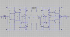
this is the version 3, a slight upgrade from version 2, with the bias controller having the collectors of the emitter followers not in series. One may say this is the orthodox version.
The low-level distorsion increase is now marginal, compared to the normal Vbe multiplier scheme. The high-level distorsion is the best, slighly better than the normal Vbe multiplier scheme.
THD with 100mV 1kHz at the input of the amplifier :
0.000024% for the normal Vbe multiplier (no decoupling cap) :
0.000698% for Soft Non-Switching 001
0.000087% for Soft Non-Switching 002
0.000027% for Soft Non-Switching 003
THD with 100mV 1kHz at the input of the amplifier :
0.000199 % for the normal Vbe multiplier (no decoupling cap) :
0.000237% for Soft Non-Switching 001
0.000187% for Soft Non-Switching 002
0.000185% for Soft Non-Switching 003
I like version 3 ! See attached .zip file. Need now to concentrate on version 3 and optimize it for :
- loading it by 2 ohm to 32 ohm, without HF instabilities
- adding a capacitor as load and getting moderate ringing on square wave
- clean overload recovery
- decent HF bandwidth
- decent slew-rate
- define the guaranteed non-switching operating range (bias current setting and bias servo loop gain setting)
- define the "bottom current" value (size of the resistor in parallel with the Schottky diode arrangement)
All this using an "old school" complementary Darlington BJT output stage.
I am now curious to see the simulation results with :
- a Vertical MOSFET output stage
- a Lateral MOSFET output stage - there may be a trouble with the 0.8V threshold voltage, quite low for biasing the emitter followers in the bias controller
- a "vintage" 2N3055 semi-complementary Darlington output stage
Those ones liking funky experiments are welcome, sending me info for building transistor-level models of the following opamps :
- µA702
- µA709
- µA739
- µA741
- LM301
- LM358
- LM1458
- NE5534
I guess that in 20 years, the amp decribed here will be considered as a nice platform for testing the acoustic signature of those unobtainable components. In 20 years, some will see value in those old opamps, like some are already seeing value in the old good unobtainable 2N3055, and more recently, some japanese vertical MOSFETS.
At the same time, some freaks will come with a redesigned bias controller, using a 3 GHz microcontroller fitted with 960 kHz 24 bit ADCs and DACs, powered by the +drive and -drive lines, taking less than one milliamp, post-stamp sized (if there are still post offices), using reatime circuit and transistor modeling, FFTs, wavelets and convolution for setting the bias in a dynamic way. You'll be able to follow his work on your TV, using WiFi. For less than 10 dollars.
Cheers,
Steph
Attachments
Last edited:
Can somebody advise how to test the temperature dependencies of the circuit described above, using LTspiceIV ?
I'm not talking about the MOSFETs parameters. I'm talking about the four Schottky and the four BJTs involved in the bias servo circuitry.
1. Is it possible to define a global temperature and make a sweep on this value, for graphically obtaining the quiescent current in function of the global temperature ?
2. Is it possible to define warm and cold zones, and see how the temperature dependency evolves ? Something like having the two big Schottky temperature 25°C above the rest of the circuit.
Thanks,
Steph
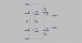
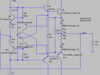
I realized that I'm late to the party, but, the attached is how to simulate temperature. I have also built the attached scheme and it works very well. Sounds good, low Thd, etc. The Schottkys don't even get warm under full load. Seems to work best with bias set above 100mA.
Ken
Attachments
I was thinking of building something similar to the attached schematic.
D382 to D385 would all be the same diode type, see attached FYPF1545DN diode datasheet (they are available from mouser).
Since they are in a plastic package, D383 can be bolted directly to D384, and D382 can be bolted directly to D385. This should provide good thermal bias stability, with no need for mounting any of the diodes on a heatsink or messing about with thermal washers.
Also, since all the diodes are the same type, and because the 4 diamond transistors are of the same type, a reasonably dependable, thermally stable automatic bias current is hopefully guaranteed.
Any comments?
Attachments
Hi klewis,
That's great news to hear that it works well in practice. How stable did you find the bias current to be? Does it vary significantly between switch-on and when the amp has fully 'warmed up'?
Thanks,
Ian
Ian, it takes a few minutes for the bias to stablize, but, then it remains quite steady. The variation between cold and warm up isn't too great.
Ken
- Status
- This old topic is closed. If you want to reopen this topic, contact a moderator using the "Report Post" button.
- Home
- Amplifiers
- Solid State
- New Class A, Super-A, Non-Switching : need a revival ?