你的线路做对了一半,实际工作时会很难控制静态电流,也会将q5损坏。
Google Translate: You do the half line, the actual work will be difficult to
control the quiescent current will be q5 damage.
Only in hard clipping does Q5 ever shut off, and I've not yet seen it run away.
In quiescence, it balances against 5.5mA pulled by R15. But this current does
create a small offset. Brought back to center by R29.
Full symmetrical circuit with twice as many Schottkys and a compliment to Q5
is less distortion, but more parts and twice voltage drop. But we speak only
a very small difference of -80db vs -100db H2 at the 1st Watt.
The idle current is about 300mA. How to reduce it ?
Change Schottky model to MBR20100CT, crosses at 100mA.
Rolling Schottkys could even become a popular pastime?!?
Add a heater and thermostat, you could regulate crossing
current with a dial. It is all silly... So long as crosses smooth
and nothing explodes, what do we care what is quiescent?
I'm also not suggesting you just totally let current run away,
but it doesn't have to be rigidly controlled. Remember we are
in rigid control of an underbias voltage instead.
Free your mind, that is an obsolete way of thinking. Emitter
log law was extremely critical the current. Little concern for
optimal crossing of this circuit. We really care only that our
square law references are crossing at the same temperature.
Independant of, and much lower temp than the output.
The diode stack should be bonded to each other for sure...
Too bad most dual Schottky packages share a common
terminal not wired for series.
Last edited:
All those patents/ideas presented here represent the various
approaches to switching problems solution. Some are better than other.
I believe, that those, that force output transistors to continiously
change the current are prefered to those, that force "nonconducting" transistor to stay at some constant DC current.
I would also suggest, that most of the solutions, typified by those
patents would benefit from supplemental Error Correction arrangement
to keep distortions in check.
I also prefer simple circuits to complex. With this in mind I would like
to remaind you, that the CORE topology of F5 (4 transistors and the
Nfeedback resistors arrangement) also exibits these properties. Usually,
the resistors ratio is selected for gain setting, but it is also affects
the amount of "non-switching" effect, and therefore, can be optimised
in that regard.
Last edited:
Could it be that kenpeter arrangement is in the same league as Dodson "Quasi-Class A / Improved Class A Bias Loop" presented at the AES 67th Convention in New-York ?
See AES E-Library: Quasi-Class A/Improved Class AB Bias Loop
See attached pictures.
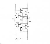
"Figure 8 is a diagram of a hyperbolic class A bias loop. Operation is such that both drivers and output devices (Dodson is talking about a Darlington output) are inside feedback loops controlled by Q1 and Q2".
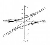
Here is a Kuroda-Dodson-Kenpeter-Cnockaert (KDKC) soft non-switching audio power amplifier with vertical MOSFETs biased at 54mA, and still Soft Non-Switching when delivering 60Vpp on a 8 ohm load. See attached pictures.
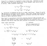
I made all base-emitter and Schottky junctions compensated. This allows setting the vertical MOSFETs bias current anywhere between 25mA and 999mA. All junctions being now compensated, one may expect a decent thermal stability. The servo-bias loop gain is now adjustable using the emitter-emitter resistor. The bigger the resistor, the softer you get the Non-Switching crossings.
Such circuit behaves gently on simulation.
The Kuroda used as reference is tricky regarding the Vbe multiplier. Of course it is not a Non-Switching circuit. The size of the decoupling cap (4.7 µF here) is critical. A smaller value like 220nF enables a fake Soft Switching, and you will see the fake by walking the current probe in the circuit, comparing the NMOS and the PMOS source currents. If you put a 47µF cap (and allow enough settling time for the .TRAN simulatoion), the fake will vanish, you will get a crude hard-switching, and you will see that the VAS current is enduring serious spikes at crossing. That's precisely and typically the illness of any "improved" Kuroda using a Vbe multiplier instead of a dumb resistor. The original Kuroda is using a dumb resistor, generates less spikes, is not a Non-Switching, and fakes (to a less extend) some smoothness when crossing.
The KDKC arrangement combines the following advantages :
0- No unobtainable nor expensive nor soon obsolete parts,
1- It eradicates all kind of crossing spikes without relying on timing capacitors,
2- It can be configured anywhere between a pseudo class-A (say 999mA Iq) and a pseudo class AB (say 25 mA Iq),
3- It is a true and guaranteed Soft Non-Switching amp, provided one properly defines the max current he is supposed to deliver, but the issue of a complex load needs to be assessed - see Benjamin AES paper about the V-I locus issue,
4- The adjustable servo-bias loop gain can be adjusted for setting the class profile anywhere between a super-soft pseudo class A (low servo loop gain, high Iq), to a mild-soft non-switching class AB (high servo loop gain, low Iq).
5- The adjustable servo-bias loop gain can be adjusted for tailoring the frequency spectrum of the individual MOSFEts source currents, a low loop gain enabling a monotonic decreasing profile of harmonics.
6- Current feedback topology (known for delivering adequate slew-rate)
7- Use the opamp of your choice, as front-end
A KDKC amp printed circuit, routed using the findings of Ed. Cherry "A New Distorsion Mechanism in Class B Amplifiers", AES 1981, would be interesting. Especially when setting it up for different class profiles, and using different audio opamp as front-end. That's bulletproof for the future.
Anyone interested ?
Cheers,
Steph
See AES E-Library: Quasi-Class A/Improved Class AB Bias Loop
See attached pictures.
"Figure 8 is a diagram of a hyperbolic class A bias loop. Operation is such that both drivers and output devices (Dodson is talking about a Darlington output) are inside feedback loops controlled by Q1 and Q2".
Here is a Kuroda-Dodson-Kenpeter-Cnockaert (KDKC) soft non-switching audio power amplifier with vertical MOSFETs biased at 54mA, and still Soft Non-Switching when delivering 60Vpp on a 8 ohm load. See attached pictures.
I made all base-emitter and Schottky junctions compensated. This allows setting the vertical MOSFETs bias current anywhere between 25mA and 999mA. All junctions being now compensated, one may expect a decent thermal stability. The servo-bias loop gain is now adjustable using the emitter-emitter resistor. The bigger the resistor, the softer you get the Non-Switching crossings.
Such circuit behaves gently on simulation.
The Kuroda used as reference is tricky regarding the Vbe multiplier. Of course it is not a Non-Switching circuit. The size of the decoupling cap (4.7 µF here) is critical. A smaller value like 220nF enables a fake Soft Switching, and you will see the fake by walking the current probe in the circuit, comparing the NMOS and the PMOS source currents. If you put a 47µF cap (and allow enough settling time for the .TRAN simulatoion), the fake will vanish, you will get a crude hard-switching, and you will see that the VAS current is enduring serious spikes at crossing. That's precisely and typically the illness of any "improved" Kuroda using a Vbe multiplier instead of a dumb resistor. The original Kuroda is using a dumb resistor, generates less spikes, is not a Non-Switching, and fakes (to a less extend) some smoothness when crossing.
The KDKC arrangement combines the following advantages :
0- No unobtainable nor expensive nor soon obsolete parts,
1- It eradicates all kind of crossing spikes without relying on timing capacitors,
2- It can be configured anywhere between a pseudo class-A (say 999mA Iq) and a pseudo class AB (say 25 mA Iq),
3- It is a true and guaranteed Soft Non-Switching amp, provided one properly defines the max current he is supposed to deliver, but the issue of a complex load needs to be assessed - see Benjamin AES paper about the V-I locus issue,
4- The adjustable servo-bias loop gain can be adjusted for setting the class profile anywhere between a super-soft pseudo class A (low servo loop gain, high Iq), to a mild-soft non-switching class AB (high servo loop gain, low Iq).
5- The adjustable servo-bias loop gain can be adjusted for tailoring the frequency spectrum of the individual MOSFEts source currents, a low loop gain enabling a monotonic decreasing profile of harmonics.
6- Current feedback topology (known for delivering adequate slew-rate)
7- Use the opamp of your choice, as front-end
A KDKC amp printed circuit, routed using the findings of Ed. Cherry "A New Distorsion Mechanism in Class B Amplifiers", AES 1981, would be interesting. Especially when setting it up for different class profiles, and using different audio opamp as front-end. That's bulletproof for the future.
Anyone interested ?
Cheers,
Steph
Attachments
-
 Dodson Hyperbolic class A & Improved class AB - AES cover.jpg78.2 KB · Views: 1,383
 -
 Dodson Hyperbolic class A & Improved class AB - fig 8.jpg33.1 KB · Views: 1,424
 -
 Dodson Hyperbolic class A & Improved class AB - fig 9.jpg52 KB · Views: 1,408
 -
 Dodson Hyperbolic class A & Improved class AB - maths.jpg84.8 KB · Views: 1,381
 -
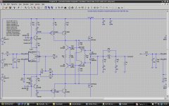 Kuroda Dodson Kenpeter Cnockaert 50mA bias TL071 60W FET amp - schematic.jpg346.7 KB · Views: 1,440
 -
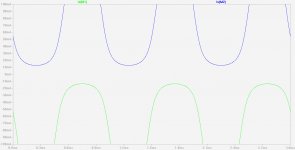 Kuroda Dodson Kenpeter Cnockaert 50mA bias TL071 60W FET amp - soft non-switching 3Vpp 8 ohm loa.jpg87.2 KB · Views: 879
 -
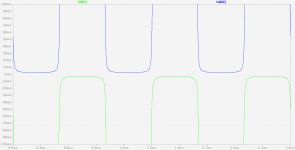 Kuroda Dodson Kenpeter Cnockaert 50mA bias TL071 60W FET amp - soft non-switching 30Vpp 8 ohm lo.jpg77.4 KB · Views: 404
 -
Kuroda Dodson Kenpeter Cnockaert 54mA bias TL071 60W FET amp.zip507.7 KB · Views: 303
Last edited:
Dodson curves on his diode. But what makes reserve current for the power device?
R1-Fig8 only seems to grant reserve current to the front transitor of the Darlington.
Is Dodson using Schottky or junction diodes here? The curve shapes are different.
If junction, might need careful regulation over the quiescent current at crossing.
OK, in the text snippet, he sais his diodes are using the Log law, so not Schottky..
If Dodson holds a Patent, I might not be able to squeak around that one. Mine is
slightly different, but is it enough different???
Last edited:
Nobody's mentioned "Erik Margan".
Regards Max Albin
Browsed the table of contents of his book "Wideband Amplifiers" on Google.
I did not see anything regarding push-pull. Just a whole lot of single ended.
am I looking to the wrong reference? Or is it buried in the text without any
specific mention in the table of contents?
Steph, what kind of voltage swing do you get out of that arrangement?
I had mine turned inside out for reason of not needing any bootstraps
nor high rails to drive the full swing. Well, 40V of 42, almost full swing...
You get less and less Voltage into 4 and 2 ohms, but that just the soft
current limiter's knee bending over at around 6A. You asked for 5A, I
don't see that happening into 8ohm unless you can swing at least 40V.
I like your expanded diamond in the center. But you gotta watch that
doesn't freak out, should it reach either rail. A pair of voltage dividers
to GND could prevent that ever happening. Even my inside-out driven
probably needs that modification too, gets wiggy when you approach
the current mirror emitter voltage, significantly less than full rail.
Maybe then I could squeeze 41 out of it? Need a volume knob to 11.
Last edited:
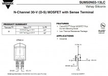
Hello, there are MOSFETs having a 4th pin called "Sense" and a 5th pin called "Kelvin".
See attached pictures. What if we put a small signal (cold) Schottky diode in series with the Kelvin terminal ? The Sense terminal voltage would then become the input of the Dodson-Kenpeter bias feedback arrangement. And no power lost.
Is the Sense output current temperature-dependent when connected to the Kelvin terminal ? Does it degrades if there is one cold small signal Schottky inbetween ?
I would like to simulate this. Is there a model available for I-sense MOSFETs ? Can somebody help me build one, if not available ?
Cheers,
Steph
Attachments
I was about to quote Margan when writing in a previous post that one should assess the behaviour of the KDKC amp on a complex load, in the context of the I-V Locus issue on the output stage.Nobody's mentioned "Erik Margan".
On the other hand, I always found Margan's Wireless World publication quite confidential, in July 1987. Of course, Ben Duncan referring it into his book is a strong asset. Margan's test rig has the advantage of simplicity. See attached picture.
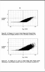
Do you know Benjamin's AES paper in 1992 ? According to me, that's the reference about the complex, changing load issue. I like Benjamin's approach. I am in search of a LTspice test rig, made according Benjamin's approach. I like the idea of I-V Locus on the output stage.
See AES E-Library: Audio Power Amplifiers for Loudspeaker Loads
See attached pictures.
Cheers,
Steph
Attachments
Last edited:
Obviously, less than what you get because mine is a source-follower one, and yours is a common-source one.Steph, what kind of voltage swing do you get out of that arrangement ?
Will you allow me trying using an opamp as front-end based on on your very interesting common-source arrangement ? I like the nearly for free and unobtrusive current limiter, on top of the improved swing capability.
But, will audio freaks love the common-source arrangement ? They will always tell you that the PSU ripple rejection is less, and that the open-loop output stage gain variation with load is more. Two negative features. Without the current limiters, there may be a risk like burning the output devices if there is a high amplitude high-frequency content, IMO.
Anyway, we should measure and compare all this, on simulation.
Cheers,
Steph
Last edited:
Allow? When did I acquire this mystic power to allow or disallow?
I personally consider any op-amp a cheat for me, since I'm still
learning. But its not a crime for others to use them. Won't make
this amplifier perform worse. And offset is much better trimmed
than discretes outside a shared package would ever match.
All that felgercarb about poor common source PSRR comes from
spanning drives with a cap, and turning sources toward the rail.
We have an active span with a high impedance. Its not gonna
impose power supply ripple upon the drive signals. What little
ripple might leak across the series impedance of two collectors?
Doesn't seem significant by comparison to the error correction.
Output stage gain variation??? I've never heard that claim before.
But lets assume for the moment it were true. Does it apply to this
case where Diodes facing the center are the virtual power devices?
Last edited:
I was about to quote Margan when writing in a previous post that one should assess the behaviour of the KDKC amp on a complex load, in the context of the I-V Locus issue on the output stage.
On the other hand, I always found Margan's Wireless World publication quite confidential, in July 1987. Of course, Ben Duncan referring it into his book is a strong asset. Margan's test rig has the advantage of simplicity. See attached picture.
Do you know Benjamin's AES paper in 1992 ? According to me, that's the reference about the complex, changing load issue. I like Benjamin's approach. I am in search of a LTspice test rig, made according Benjamin's approach. I like the idea of I-V Locus on the output stage.
See AES E-Library: Audio Power Amplifiers for Loudspeaker Loads
See attached pictures.
Cheers,
Steph
Keith Howard also had a very good article on SOA and the difficulty of driving speaker loads in Stereophile about a year ago.
Cheers,
Bob
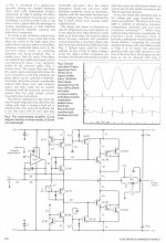
My schematic above, for those too lazy to open LTSpice...
1st proposal: Up for comments, suggestions, dirty jokes...
I'm rather proud to see it swings 40V with only 42V rails.
Beat it or join it...
Miller effect in the CS output stage will kill you, especially since the gate-drain capacitance is highly nonlinear in the MOSFETs, and gets to the range of 500-1000 pF at Vgd around 1V. If you "forward bias" the gate-drain electrodes (gate voltage more positive than drain voltage on an N channel device) the capacitance skyrockes further. Take a look at the IRFP240 datasheet.
Cheers,
Bob
At fisrt glance, the Ben Duncan books looks quite general. Digging into the individual chapters, the big and positive surprise is to realize how precise and accurate Ben Duncan is. The appendixes are unvaluable, plenty of references, plenty of historical info. Many many thanks for pointing this great source of info !
Page 133, about the non-switching amplifiers, it reads :
"This involved a kind of positive feedback, and carrying the risk of blowing-up the output stage ! It also relies on the switching of small diodes, which ameliorated and displaced, rather than overcoming the switching problem".
I guess Ben Duncan didn't wanted to write explicitely that the Technics SynchroBias, marketed as "New Class A", was displacing the problem instead of solving it. The Technics "New Class A" is thus a little bit apart. It should be clear and remembered that JVC "Super-A", Pioneer "Non Switching" and Sansui "Tanaka Non-Switching" are not relying on diodes to be switched.
It is amazing to see the LT1166 biasing integrated circuit, being ignored. Were there commercial power amplifiers using a LT1166 biasing integrated circuit ?
Like Margan, what's worrying me is the behaviour of the output stage when driving a complex load like a loudspeaker. Some optimizations like the ones discussed here may prove unable to cope with capacitive, inductive, or varying impedance loads, especially on non-periodic, non-static, non-symetric input signals like music is. In this context, is there a LTspice standard test gig I can use, for better knowing the behaviour of the output stage ?
Cheers,
Steph
I think the LT1166 is a great part. It is an elegant non-switching solution that eliminates the bias trim pot. However, the arrangements that use it in the app note are not all of really low-distortion. One needs to not run the audio signal through the LT1166, but instead use it purely as a dynamic bias spreader. Miller compensation of the amplifier then gets interesting because the signals at each end of the LT1166 bias spreader are nonlinear. Also, compensating the LT1166 itself in some arrangements can be a bit tricky. These are probably some of the reasons why it has been overlooked by some.
A further avantage of the device is that it is a real-time adaptive bias controller, minimizing the thermal bias mis-tracking distortion that plagues many BJT output stages.
Cheers,
Bob
Miller effect in the CS output stage will kill you, especially since the gate-drain capacitance is highly nonlinear in the MOSFETs, and gets to the range of 500-1000 pF at Vgd around 1V. If you "forward bias" the gate-drain electrodes (gate voltage more positive than drain voltage on an N channel device) the capacitance skyrockes further. Take a look at the IRFP240 datasheet.
Cheers,
Bob
I hoped by same mechanism that provides reserve current, I've kept gate
charge from plummeting uselessly after cutoff. I'm aware any drive too far
into conduction or cutoff takes an ever increasing charge to make change
in channel current. Is this the same hazard you warn of? You seem to go
further than this, to warn specifically about when Drain is less than Gate???
It plots a pretty decent almost rail to rail sine wave at 96KHz in the sim.
You suggesting a capacitive challenge LTSpice has not accounted for?
This effect is not represented in the model?
Its no big deal to make a change to bipolar, if that would work better.
I already posted an example with PNP Darlington substituted for the
MOSFETs on the P-CH side only. Was to prove the diode was making
the complimentary curves, and curves did not rely upon the power
device. But illustrates swap for BJT is a do-able thing, even easy...
You forsee any new challenges if the power devices were Darlington?
Last edited:
I don't see anything bout what happens to gate charge
below VDS<40? Maybe you got a more complete version
of the spec sheet than the one I'm looking at??? The
trend in Fig 6 almost seems to suggest Qg goes down
slightly as drain voltage decreases from 160 to 40, but
that makes no sense, or does it??
I do not doubt for a second what you are telling me is
more accurate than any spec sheet. All the same, I'm
rather confused by it???
Attachments
Last edited:
I don't see anything bout what happens to gate charge
below VDS<40? Maybe you got a more complete version
of the spec sheet than the one I'm looking at???
I do not doubt for a second what you are telling me is
more accurate than any spec sheet.
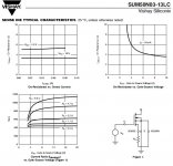
Your datasheet says 1300pF for VDS 25V and Vgs 0V..
I suppose that Bob did made some real world measurements..
Well, whats confusing to me is that Bob makes it sound so much worse
for the common source configuration. Yet Qg + Qdg sum up the same
either way you go. If I can charge and discharge those Coulombs in the
required timeframe, does the apparent capacitance change matter?
The drive circuit can source or sink 5.5mA into the gate(s), and that
seemed plenty fast enough on the simulation for the output voltages
and currents and bandwidth we were trying to achieve.
I just want to know if his warning refers to something the simulation
is not telling us? I don't take anything Bob sais lightly. Aim to be the
next Bob Cordell after he's dead. But untill then, Long Live the King!!!
If he sais this is not going to work, I want to fully understand why?
The amplifiers I final test every day are Class-D EVMs, and designed
by someone else. I'm not even in the loop on the design side. My real
world hands-on experiences may not be relevant to what I actually
need to know to design a flawless class AB amplifier. I am not above
making clueless mistakes.
Last edited:
- Status
- This old topic is closed. If you want to reopen this topic, contact a moderator using the "Report Post" button.
- Home
- Amplifiers
- Solid State
- New Class A, Super-A, Non-Switching : need a revival ?