O don't really understand you.
I always learned (with the few electronic lessons at study of physics) that there only can be current flowing to the base of a transistor, not from the base of a transistor.
The emitter (or collector with PNP) would be the current from the collector + the (very little) current from the base.
So why should there be current flowing from the base of Q1/Q2 though the diodes etc ?
Or do I miss a point ?
edit:
Or do you mean that the opamp must deliver to much current, but that there is current flowing in the opposite direction, so the sum will be low ?
A 100-200ohm resistor at the output of the opamp will work ?
Hi,
an NPN transistor has current flowing into the base.
The Emitter Current = Collector current + base current.
A PNP transistor has current flowing out of the base.
The Emitter current = Collector current - base current.
But, it's not just about the directions of the base currents.
The collector current of the upper driver can only be sourced from the base of the upper output device. The base current is very much dependant on the output current and so the driver is going to see a variable collector current and as a result it will not amplify linearly, if it works at all. There is a missing resistor. That's why I asked
The same applies to the lower driver.does the compound follower pair (CFP) work if the collector resistor on the driver is omitted?
So a resistor (with the same value as R3?) from base from Q2 (net6 and output opamp) will do the trick ???
If that is the case, it will be funny, because I found it strange that the schematic from ESP (and thus mine) is not symmetrical.")
(variable resistor in the diode chain would be better I think if we put another resistor on the negative site ???)
So this is what you mean?
If that is the case, it will be funny, because I found it strange that the schematic from ESP (and thus mine) is not symmetrical.
(variable resistor in the diode chain would be better I think if we put another resistor on the negative site ???)
So this is what you mean?
An externally hosted image should be here but it was not working when we last tested it.
Hi
The idea of push pull is that one polarity transistor turns on while the other turns off. When a transistor is turned on, in order for it to turn off in a respectable amount of time, it requires some way to deplete the charge from the base, at least a resistor between the base and emitter. IOW, the way it is now, Q3 & Q4 will cross conduct and blow out. Q1 & Q2 collector current equals the base current from Q3 & Q4 and this is way too small a current for Q1 & Q2 to operate, the other reason for a resistor from base to emitter.
Question: If the output of the op-amp is placed on the bases of Q1 & Q2, and the output is fed back directly to the emitters, +/-15V for the op amp, +/-20V for the output, do you see the problem with getting rail to rail swing from the output? Also, if the gain of the CFP is set to unity, it may be difficult to get stability and keep it from oscillating. (In addition you need gain to get to rail to rail +/-20V) Generally, this type of stage would have a voltage divider to set the gain of the CFP. A feedback resistor from output to the emitters of Q1 & Q2, and a resistor from the emitters to gnd. If gain isn’t desired, a follower instead of a CFP would be a better solution.
It may work as is in the simulator, but it won't work that way in real life.
The output from the op-amp can't be higher than 15Vp. With unity gain of the CFP, you can't get a larger signal than 15Vp from the output. But if this is desired, then why use +/-20V?
Don't know what happened with the posts...
Anyway......a few moments......
for Q1, Q2, think of the base as the + input and the emitter as the -input.
Don't know what happened with the posts...
Anyway......a few moments......
for Q1, Q2, think of the base as the + input and the emitter as the -input.
Attachments
That may be an attempt to keep the transistor away from saturation, but it should not saturate until below 1 Vce. 5V above the peak output of 15V seems like a bit of a waste, eh?
It appears the LM388 is a power amplifier designed to work from a single polarity supply, not a power supply, unless I'm reading the datasheet wrong.
It appears the LM388 is a power amplifier designed to work from a single polarity supply, not a power supply, unless I'm reading the datasheet wrong.
I used 10k for the extra resistors you're talking about, is that a reasonable value ?
For the LM338 supply:
http://www.elecfree.com/electronic/...8/03/power-supply-20v-and-20v-5a-by-lm338.gif
This construction was also here on diyaudio.com a time ago.
Will that work properly?
For the LM338 supply:
http://www.elecfree.com/electronic/...8/03/power-supply-20v-and-20v-5a-by-lm338.gif
This construction was also here on diyaudio.com a time ago.
Will that work properly?
I have not seen that chip used that way, but it resembles the LM317 circuit. Build it and find out
If you are reffering to the base to emitter resistors for Q3, Q4, there will only be the Vbe (0.6V) voltage of those transistors across the resistors. 0.6V/10,000 = 60uA. Q1 & Q2 being BD139/140 needs a bias of several mA. It is possible (and probably better) to use small signal devices here but they will still need a few mA of bias. 0.6V/200 Ohms = 3mA So more like around 200 Ohms. 180 Ohms or 220 Ohms, whatever you happen to have on hand.
If you are reffering to the base to emitter resistors for Q3, Q4, there will only be the Vbe (0.6V) voltage of those transistors across the resistors. 0.6V/10,000 = 60uA. Q1 & Q2 being BD139/140 needs a bias of several mA. It is possible (and probably better) to use small signal devices here but they will still need a few mA of bias. 0.6V/200 Ohms = 3mA So more like around 200 Ohms. 180 Ohms or 220 Ohms, whatever you happen to have on hand.
Yes, Andrew is correct, you have to have a seperate secondary for this to work unless you have a negative voltage regulator circuit for the negative side. These are simply not as common, so the seperated secondary regulator circuit in post 52 is more often used.....same result.
because the simulator is answering your wrong questions.b_force said:mm with those two 220ohm resistors on that specific place (and the same circuit) the performance is worse.
How can that be ?
b_force said:mm with those two 220ohm resistors on that specific place (and the same circuit) the performance is worse.
How can that be ?
In what way?
There is also a very big different when a put the opamp output between D1 and Rvar2, D1 and D2 or D2 and Rvar1.
Which one van I use?
Wonder how it would work paralleling resistors with D1, D2?
maybe like 330 Ohms? Op amp output between the resistors (D1, D2)
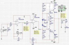
Here is a new update, maybe will that be more clear.
The opamp is now connected between the two diodes.
First, at post 44, the opamp was connected between the lower diode and Rvar.
Any further improvements/comments on the schematic ?
An externally hosted image should be here but it was not working when we last tested it.
The opamp is now connected between the two diodes.
First, at post 44, the opamp was connected between the lower diode and Rvar.
Any further improvements/comments on the schematic ?
- Status
- This old topic is closed. If you want to reopen this topic, contact a moderator using the "Report Post" button.
- Home
- Amplifiers
- Solid State
- Little opamp/darlington amplifier