Distortion analyser = great soundcard ")
I'm using a Asus xonar D1, which can measure up to 0,0007% (loop test with RMAA and ARTA). (I prefer ARTA because it can test THD, IMD with different kind of test noise/sine etc etc)
also the EMU1212M is a very well performing card. (all depends on the A/D and D/A)
I;ve measured a few amplifiers with it and it was almost the same value as the value which where given in the specs/parameters.
But maybe I can try first a bit simpler design (less critical goals) to start with and than improve the whole thing.
(can't find the wave generator ??)
I just want to remind you that there is a difference between a plain number and accuracy. You always measure THD+noise and I doubt that your soundcard really can measure at these low levels. At least I would not trust the results.
I don't know what kind of amps you tested, but most do not specify into which load for example the THD at 1kHz is obtained (big factor!). And wether filters where used, what the measuring bandwidth was, wether noise was subtracted.
Not really reliable, in my opinion.
Have fun, Hannes
I don't know what kind of amps you tested, but most do not specify into which load for example the THD at 1kHz is obtained (big factor!). And wether filters where used, what the measuring bandwidth was, wether noise was subtracted.
Not really reliable, in my opinion.
Have fun, Hannes
All measurements where done with an 8 ohm load, 20-20kHz en different kinds of output power. (1W - 10W - 20W usually or starting with 2,83V)
I almost got the same results of the datasheets or specs.
Off course it's true that it al depends on your accuracy, but with several test you can get a decent result.
But I'll look further and improve the concept
Which (standaard) transistors can I use for decent performing BD139/140 and BD438/437 ? (or BD533/534)
All right, still learning, but this would be the new idea.
Added a second opamp for volume control, both inverted (so the output will be non-inverted)
Any comments/helpfull advise ?
Would it be better if I let both opamps amplify ?
Added a second opamp for volume control, both inverted (so the output will be non-inverted)
An externally hosted image should be here but it was not working when we last tested it.
Any comments/helpfull advise ?
Would it be better if I let both opamps amplify ?
it won't work, the output transistors will be destroyed immediatly after power on!Any comments/helpfull advise ?
regards
I would recommend Jung's multiloop approach - the LT1210 is a T0-220 packaged CFA amp with 1.1 A typ output that could handle the power with heatsinking
wrapping a low distortion op amp around 2x LT1210 in parallel (small current sharing resistors) should get you there as far as active device performance is concerned
as mentioned layout and possibly parts selection could further limit distortion performance even if the topology/active devices are capable - biasing the 2 LT1210 outputs against each other in push-pull Class A reduces some layout and PS related distortion mechanisms that could be a problem for the inexperienced
LT1210's are pricey - but for a one-off it shouldn't be a concern
a little specialized knowledge may be required to assure the loop is stable - it helps using a output buffer/gain stage that's faster than the outer low distortion op amp GBW (or rather loop gain intercept) which is where the CFA output op amps help
more sophisticated compensation could get the performance from the cheaper audio chip amps ( LM3886 and similar) with the outer loop low distortion op amp feedback at 1KHz but their low speed and minimum gain requirements make the design more difficult
Juergen Knoop said:the output transistor will multiply the driver transistors current.
There is no stable setting possible because of parameter spreads and temperature dependence.
The circuit may work in sims with ideal parts, but in reality the transistors will just blow.
regards
Ok, I understand it a little bit.
The circuit I had maid, is just a little bit different than the circuit on ESP site. But what is the big difference ?????
I just have a pair BD437/436 laying around (and also the 5x numbers), so why not use it ?
(I changed R3 from 100K tot the standard 2,2K also with de Rvar underneath it)
euhm ??
I'm really sorry, but I don't see the difference between:
and:
Except for some different values of resistors etc
And the inverting opamp
I'm really sorry, but I don't see the difference between:
An externally hosted image should be here but it was not working when we last tested it.
and:
An externally hosted image should be here but it was not working when we last tested it.
Except for some different values of resistors etc
And the inverting opamp
Juergen Knoop said:aah, I see...
regards
Little mistake ? So, how does it look ?
series emitter R helps stabilize output stage bias
- adding 0.2- .3 Ohm in each emitter and adding a diode to the bias string will give a much more robust bias
if the emitter R becomes too large there can be probelms if you have to drive really large Cload (long cable?)
if you don't have any DC signal component then bootstrapping the diode bias resistor midpoint with a large C to the output is good for lowering op amp load/distortion too
Sziklai/CFP composite output transistors can give low distotion if biased Class A, b-e resistors to the rails on the output Q inputs are really necessary for decent performance
Jcx, thank you for your useful advise and tips.
Can you explain a little bit more what you mean ?
(maybe with the numbers from my schematic)
I understand that there must be 0,2-0,3 ohm resistors from emitter of each transistor.
So that will be Q3 and Q4 to VEE/VSS
And Q1/Q2 to Rload.
With the bias string you mean the two diodes D1 and D2 I think
Also a (huge) capacitor from net 10 to the transistor(s) ?
Hi,
does the compound follower pair (CFP) work if the collector resistor on the driver is omitted?
I can see the only source of current for the driver is from the base of the output device and this current will vary with output current. That does not sound too clever.
Where does the current from the V+ through R3 and D1&2 go to? Surely it can't all go down the 2132 output.
In the same vein, where does the base current of Q2 go?
yes, I didn't see the driver-output connection, making it a compound stage.b_force said:
So, how does it look ?
So my apologies for expecting always the worst from other people!

I don't have a clue about this circuits performance.
But for the ease of mind, I would prefer a beefed up ESP project 113.
Those circuits are quite standard and known to be working.
Regards
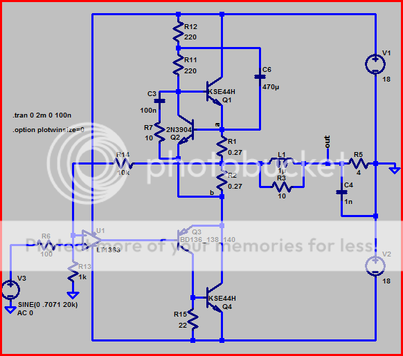
shows some of the points mentioned:
Q3,4 Szilkai/CFP compound transistor requires R15 - sized to bias Q3 into Class A with worst case estimate of Q4 Ib, also to turn off Q4 fast and remain in linear operating mode - Q3 may require a little heatsinking, Q1,4 require good heatsinking
R11,12+C6 is a AC bootstrapped current source for the bias regulator Q2
current regulated output bias only good for push-pull Class A - limits hard on one side so set the bias high enough to stay Class A with any load/waveform combo - but worth it according to sim - lower distortion than diode string
C4 sims cable load capacitance, for 1nF the L1,R3 HF decoupling network is needed for stability
at >5 MHz loop gain intercept and 50 MHz ft transistors this would need good layout and ps bypassing, you may encounter further high frequency issues not simmed
the usual LtSpice SWCADIII file, remove .txt extension
Attachments
All right, this would be the new schematic.
The bootstrap capacitor would be between R3 and Rvar (net 18) and R9 and R5 (net 16)
But I noticed that it also requires a lot more current.
(the same thing with a third diode)
The total THD now simulated is extremely low (around 0,0006% @ 22kHz and at 1kHz something in the 10^-5)
An externally hosted image should be here but it was not working when we last tested it.
The bootstrap capacitor would be between R3 and Rvar (net 18) and R9 and R5 (net 16)
But I noticed that it also requires a lot more current.
(the same thing with a third diode)
The total THD now simulated is extremely low (around 0,0006% @ 22kHz and at 1kHz something in the 10^-5)
- Status
- This old topic is closed. If you want to reopen this topic, contact a moderator using the "Report Post" button.
- Home
- Amplifiers
- Solid State
- Little opamp/darlington amplifier