AndrewT said:Hi Xpro,
any chance you could post the original with a translation?
ps,
I can't even see the Kulish in all that complexity!
Hi Andrew,
I would ask his permission to do that - if he's OK with the translation I will do it.
Cheers
Alex
linuxguru said:Yup - way too complicated. Also, there is an error in the diagram - Vt4 and Vt6 emitter arrows seem to be inverted.
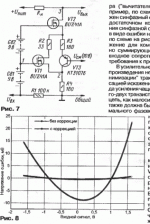
Yes, it is an obvious error - these should be NPN. I've sent a PM to Kulish and it he replies positively I'll translate the full article. He's got another interesting EC circuit there. Here is the picture:
Cheers
Alex
P.S. - The graph shows the error voltage (in mV) re. input voltage in V for non-corrected and corrected circuits.
Attachments
It is somewhat difficult to see a stringent reason for this hype.
Fourier analysis of some function is ok. but the function itself is a mere approximation.
I'll bet and probably won't loose when I say there is no method of
"error correction" with differential amps that has not been inventend from 1935 to 1950 in the course of development of Radar echo receivers. That is an application where accuracy matters.
Which kind of accuracy matters in audio amps is an open question. For example some psychological test performed in 1980 or so has shown that professional musicians almost unanimously preferred a particular loudspeaker and just this had a 30% H2
peak at 400/sec. But these profs also detected within a minute when one tweeter out of 12 in a dodecahedron case tweeter unit had failed.
So after all I'll still buy THDs for 10 cent on the dollar.
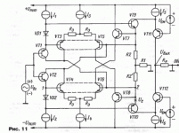
Some reverse engineered circuit analysis
Some reverse engineered circuit analysis, FWIW ;-)
See attached, originally posed by Alex (x-pro)
Basic circuit operation
First - ignoring the 2 LTP error correction amplifiers (VT3+5,VT4+6 and their cascodes VT7 & 8), the circuit operates by applying a fraction of the input voltage across R1 and thus altering the current in VT9 & VT10 in proportion to the input voltage. VT9 & VT10's bias current is determined by VD1+VD2 voltage across R2 and R2' each half being summed with the current from I1 and I2 respectively. I5 / VT11 and I6 / VT12 are folded cascodes developing output voltage across Rm.
VT1 & 2 are current sourced emitter followers, fed from I1 and I2. VT9 & VT10 bases track the input voltage ~ +/- 2 * 0.65V. The major error occurs due to the variation of Vbe with varying collector current in VT9 & VT10 - since Vbe in VT1,VT2 & VD1,VD2 are near constant due current sources I1 & I2.
Error correction
The error adjustment occurs in VT3,4,5 & 6. For VT4 & VT6 the difference between points 1,2 is due to the Vbe voltage change in VT10 due to the variations in current plus the intrinsic emitter resistance. An identical argument applied to VT3 & 5 with the Vbe changes in VT9.
For a +ve input swing, the current in VT10 falls since the junction of R2 / R2' / R1 goes +ve. This results in a Vbe change (reducing) causing point 2 to shift slightly less +ve, with respect to point 1, forcing VT6 to conduct less while VT4 conducts more - ending up in VT9's emitter. Ultimately, this error causes slightly too much current in VT10 and hence slightly too little in VT12. By symmetry with VT3 & VT5, VT3's collector current will decrease compensating the the original error of too much current in VT10. R3 adjusts the gain of the LTP's to 'exactly' trim the level of correction.
NOTE
The bias current in VT9 & VT10 also includes ~1/2 of the tail current in the 2 LTP's, the other half of the LTP's tail current get dumped to the rails through VT7 & VT8. In my simulations, it was not possible to exactly balance the LTPs ...
Is it feedback ?
No . Errors cause an adjustment current to be developed which is isolated from the input although there is degenerative feedback in the LTP's (R3)
/dave
PS - i'll post a LTSpice model if anyone would like it
Some reverse engineered circuit analysis, FWIW ;-)
See attached, originally posed by Alex (x-pro)
Basic circuit operation
First - ignoring the 2 LTP error correction amplifiers (VT3+5,VT4+6 and their cascodes VT7 & 8), the circuit operates by applying a fraction of the input voltage across R1 and thus altering the current in VT9 & VT10 in proportion to the input voltage. VT9 & VT10's bias current is determined by VD1+VD2 voltage across R2 and R2' each half being summed with the current from I1 and I2 respectively. I5 / VT11 and I6 / VT12 are folded cascodes developing output voltage across Rm.
VT1 & 2 are current sourced emitter followers, fed from I1 and I2. VT9 & VT10 bases track the input voltage ~ +/- 2 * 0.65V. The major error occurs due to the variation of Vbe with varying collector current in VT9 & VT10 - since Vbe in VT1,VT2 & VD1,VD2 are near constant due current sources I1 & I2.
Error correction
The error adjustment occurs in VT3,4,5 & 6. For VT4 & VT6 the difference between points 1,2 is due to the Vbe voltage change in VT10 due to the variations in current plus the intrinsic emitter resistance. An identical argument applied to VT3 & 5 with the Vbe changes in VT9.
For a +ve input swing, the current in VT10 falls since the junction of R2 / R2' / R1 goes +ve. This results in a Vbe change (reducing) causing point 2 to shift slightly less +ve, with respect to point 1, forcing VT6 to conduct less while VT4 conducts more - ending up in VT9's emitter. Ultimately, this error causes slightly too much current in VT10 and hence slightly too little in VT12. By symmetry with VT3 & VT5, VT3's collector current will decrease compensating the the original error of too much current in VT10. R3 adjusts the gain of the LTP's to 'exactly' trim the level of correction.
NOTE
The bias current in VT9 & VT10 also includes ~1/2 of the tail current in the 2 LTP's, the other half of the LTP's tail current get dumped to the rails through VT7 & VT8. In my simulations, it was not possible to exactly balance the LTPs ...
Is it feedback ?
No .
Errors cause an adjustment current to be developed which is isolated from the input although there is degenerative feedback in the LTP's (R3)/dave
PS - i'll post a LTSpice model if anyone would like it
Attachments
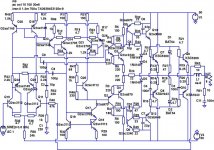
OK, I'm back with a more elaborated topology - actually, practically a full topology of a Class A/AB/B power amp capable of 100 W +. As shown, it is biased to Class AB, almost at the edge of pure Class B operation. It simulates with H2 ~= H3 < -105 dB, corresponding to THD ~= 0.0005% at ~40V amplitude Vout swing. Other harmonics are all lower than -115 dB. As always, distortion figures should be taken with a generous pinch of salt, and these are sensitive to the type of transistor and the specific model used.
The input stage is an elaborated version of one posted earlier by Bob Cordell (I'll dig out the reference later) - in particular, the use of active loads for the LTP biased from a pair of voltage followers that are also buffers for the next stage is Bob's little gem of an idea. I improved on it a bit by using a Sziklai/CFP for the input LTP - this has bounded gain, set by emitter-degeneration and cross-collector load.
The VAS is a 'Hitachi' topology, again improving on Bob Cordell's idea above. Bob's original topology used PNP VAS transistors. These were buffered by PNP voltage followers with their collectors grounded, a la Douglas Self - I decided to put the collectors to good use to develop differential voltages across collector loads to drive a pair of NPN Sziklai/CFPs instead. These, in turn, reflect their current with a traditional NPN Wilson current mirror to develop a voltage swing which drives the Kulish-corrected power stage (which is an elaborated version of the ones I posted earlier). The bonus of this topology is that all 3 transistors in the VAS that dissipate relatively higher power (Q14, Q17 and Q21) are NPNs - for which a number of commodity transistors (e.g. 2sc3423, KSC3953, ...) are suitable.
The schematic is a bit hard to read, mainly because of artifacts related to the way LTSpice generates an image - it generates a .wmf, which I have to reduce 1:2 and convert to a .png, to upload here. I've also skipped the FFT plots and the LTSpice .asc files. As always, this is still very much work in progress.
Notes:
1) C8 and C9 provide dominant-pole compensation. R2 and R59 provide some lead compensation and help roll off some HF gain in the first two stages. They can be tweaked (within limits) to change the sonics, e.g. to adjust the ratio of H2:H3. As shown, H2 ~= H3.
2) VAS slew rate is bounded by the LTP tail current divided by Cdom - here it's about 2 mA / 100 pF ~= 20 V/usec.
3) It can be driven to higher than +/- 40 V at the output, with onset of clipping dependent on various bias voltages, generally above 46 V.
4) At low swings (Vout of < +/- 5 V), H2 and H3 fall below -110 dB region. The output stage has to be biased to the edge of Class B, or fully in Class A operation to get good THD numbers - it falls off a bit in the middle of Class AB.
Edit: Upload of .png or .pdf not working - I'll try to upload the schematic later in the evening.
linuxguru said:The schematic is a bit hard to read, mainly because of artifacts related to the way LTSpice generates an image - it generates a .wmf, which I have to reduce 1:2 and convert to a .png, to upload here. I've also skipped the FFT plots and the LTSpice .asc files. As always, this is still very much work in progress.
looking forward to see the schematics. BTW, LTSpice allows you to "copy bitmap to Clipboard" - then you can just paste it into a picture editor and save as GIF or PNG so there are no artefacts.
Cheers
Alex
linuxguru said:The option to copy bitmap to clipboard is grayed out when running LTSpice using Wine under Linux, like I do. That leaves only the .wmf option.
Another try at uploading the schematic...
You might just do a screen capture and use GIMP to resize/crop it. Then save as JPG.
Edit: Made it out finally. I exported a .wmf, then opened it in Gimp, scaled it by 2/3, and then wrote it out as a .jpg with fairly high compression to get below the 100k limit here. That seems to be the best quality image so far, although .png also works.
Attachments
>similiarity with Edmond's local NFB output stage
Link to diyaudio thread/post please? Mine uses local NFB, for sure - voltage-series feedback to the Kulish transconductance cells, in addition to local CFP feedback and emitter degeneration.
> compared if it is ordinary 2 or 3 EF darlingtons?
Compared to a plain Class-AB Self Type-II EF, I'd estimate that this gains about 20-40 dB on THD20 numbers, other things being equal. The big gain is on clobbering H3 drastically, below H2 with some tweaking on the compensation.
Most of the additional expense is on inexpensive passive components and small-signal transistors, so it's worth the added complexity.
> R2 and R59 provide some lead compensation
Correction: that should read 'C2 and R52 provide some lead compensation'.
Link to diyaudio thread/post please?
http://www.diyaudio.com/forums/showthread.php?postid=1374791#post1374791
As I understand it, Edmond's core is Q2-Q3, as they sense the output node (via 500ohm resistors), compare it to input/base, and transmit the error difference to current mirrors.
In your output stage, Q2-Q3 is replaced by Kulish cell, is this right?
> In your output stage, Q2-Q3 is replaced by Kulish cell, is this right?
My topology is indeed superficially similar to Edmond's error-correcting topology that you referenced. He uses a single BJT with degeneration (for each half) as a transconductance device, and transfers the current using current mirrors to eventually generate the voltage output drive, to MOSFET output devices in his case.
Mine uses Kulish cells (which are far more linear than single BJTs with degeneration, as transconductance devices) instead of Q2/Q3, and transfers the currents through Sziklai current amplifiers to the output devices, which are BJTs and therefore only require current drive.
Edmond's use of a current mirror is a very nice touch - I could try that, but the impedance of the input side of a current mirror may be too low to use as a load to a Kulish cell. It's worth simulating it, however.
The advantage over Edmond's topology is that all elements can be chosen to be more linear - the BJT as a pure current amplifier has a hfe dependence on Ic, but with careful choice of devices, this can be minimized. In particular, the 2sc5200/2sa1943 output pair have ultra-flat hfe over a wide range of Ic. That leaves only the predrivers/drivers as a contributor to non-linear current amplification, and this can be minimized with a good choice of BJTs. My choice was primarily driven by availability and accuracy of the Spice models, but various other choices exist:
Possible choices for pre-drivers:
2sa970/2sc2240
2sa1016/2sc2362
2sa1191/2sc2856
2sa1049/2sc2459
...and many others.
Possible choices for drivers:
2sb649/2sd669
2sa1930/2sc5171
2sa1112/2sc2592
2sa1535a/2sc3944a
...and many others
As I stand pat that a good amp should reproduce the emotional content of music and as I have little interest in more or less complete simulation I simply built two Kulish cells driven by long tailed pair and added a relay switch thus I could compare the performance with the standard amp, a SRPP driven by long tailed pair, as last stage of preamp feeding the power amp.
Although admittedly subjective ( what else ever heard objective music - that's impossible ) the "sound" of the Kulish appeared
harsh and unpleasant at higher levels yet somehow more transparent at low levels than the respective SRPP.
The power amp requires 1.5 volts rms into 22 kOhms.
I don't have reliable equipment for more exact measurement.
A soundcard reading a 8 kbyte wavetable to produce sine and
a soundcard running spectrum analyzer boosted a bit by a switched capacitor filters set to suppress the first harmonic
makes a first guess.
I assume that Kulish correction excels only at H2 and H3 and fails incrementally for higher harmonics.
But just these determine the overall impression while H2 and H3
do not besides that loudspeakers produce especially H2 in the 5% range.
The Kulish can be regarded as a small-signal transconductance structure - basically, a more linear small-signal FET than a real one. It does best with certain ranges of gains, and certain ranges of load impedances; but in those sweet spots it is unbeatable at what it does best - ultra-linear conversion of voltage to current.
There's nothing to prevent it being used as another building-block to develop a larger topology, alongside existing and proven structures and mechanisms. That's what I tried to show in the Class-AB example above.
There's nothing to prevent it being used as another building-block to develop a larger topology, alongside existing and proven structures and mechanisms. That's what I tried to show in the Class-AB example above.
(OT) LTSpice under linux / wine
linuxguru,
you can try "wmf2eps" to convert WMF files to postscript then use "ps2pdf" to convert postscript to pdf files for posting, eg:
wmf2eps --ps --centre --maxpact -o draft.ps draft.wmf
ps2pdf draft.ps draft.pdf
this seems to work for schematics but is useless for fft's
packages needed : libwmf & ghostscript
dave
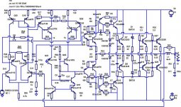
Another update on the same topology, with some modifications/optimizations to improve the THD20 numbers in LTSpice - it now simulates with H2 ~= -119 dB, and H3 ~= -117.5 dB, and everything else below -125..-130 dB. It looks like I've hit a brick wall here with H3; the last 2.5 dB to get to -120 dB is proving elusive (it's fairly easy to make H2 dominate H3 by increasing the value of C8, but both will increase and make the THD20 numbers worse). These numbers are at approximately +/- 40 V output swings, corresponding to 100W into 8 ohms, Class-AB almost at the edge of Class B. At lower swings, the harmonics almost vanish.
Once again, apologies for the quality of the image:
Once again, apologies for the quality of the image:
Attachments
- Status
- This old topic is closed. If you want to reopen this topic, contact a moderator using the "Report Post" button.
- Home
- Amplifiers
- Solid State
- Kulish Corrector for Class-A EF O/P Stage