x-pro,
I know that feedforward focuses on the promise of the future rather than feedback which corrects mistakes of the past but this is true in business, human behavior, etc. where such a mental visualisation of the process could help the understanding.
In feedback theory (I don't know if a "feedforward theory" realy exist) this concept of feedforwarding could be accomplished or equivalate simply moving a member from one part to the other of the equation. Or, in the flow description, by changing order of some processing blocks, etc. Feedforward is completely described using feedback concepts.
So even this Kulish circuit could be re-draw to have been seen as a simple circuit with feedback. Not a big deal.
There are no "NFB-based circuits" in electronics. Maybe there are some no global feedback circuits. Local feedback exist in any circuit which use active components because all those active devices are nonlinear by nature.
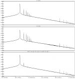
The cancellation of error can be seen in the attached fft.
The top two traces show the collect current fft of the two transistors.
Cancellation occurs when these currents are combined, in appropriate proportions, in R3 / R4. This is show in the lowest trace - which is, of course, the output voltage
The top two traces show the collect current fft of the two transistors.
Cancellation occurs when these currents are combined, in appropriate proportions, in R3 / R4. This is show in the lowest trace - which is, of course, the output voltage
Attachments

Hi
I would agree that the terminology in my previous message was perhaps not precise enough") . And I would agree that it is very difficult to find a circuit without at least a local feedback (and in the case of "Kulish Cell" such local feedback is obviously present in a form of an emitter degeneration. However there is no global NFB in that circuit - there is no path (except usual parasitics) from the output back to the input. Linear transfer function here results from combining two unlinear transfer functions. It is clear from the simulation as both transistor collector currents are very distorted, but their sum is almost distortion-free. As DRC noted earlier, this circuit requires a fine tunung for minimum distortion.
. And I would agree that it is very difficult to find a circuit without at least a local feedback (and in the case of "Kulish Cell" such local feedback is obviously present in a form of an emitter degeneration. However there is no global NFB in that circuit - there is no path (except usual parasitics) from the output back to the input. Linear transfer function here results from combining two unlinear transfer functions. It is clear from the simulation as both transistor collector currents are very distorted, but their sum is almost distortion-free. As DRC noted earlier, this circuit requires a fine tunung for minimum distortion.
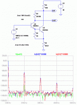
I would like to challenge you to find an NFB connection from the output in the original Kulish circuit. In the attached picture is the circuit and FFT plot for the output and two collector currents (scaled for convenience). Simulated THD result is about 0.0012% at 10 kHz and 0.5V input. At the same time the THD of Q1 collector current is 6% and the THD of Q2 collector current is 0.47% .
Cheers
Alex
I would agree that the terminology in my previous message was perhaps not precise enough
. And I would agree that it is very difficult to find a circuit without at least a local feedback (and in the case of "Kulish Cell" such local feedback is obviously present in a form of an emitter degeneration. However there is no global NFB in that circuit - there is no path (except usual parasitics) from the output back to the input. Linear transfer function here results from combining two unlinear transfer functions. It is clear from the simulation as both transistor collector currents are very distorted, but their sum is almost distortion-free. As DRC noted earlier, this circuit requires a fine tunung for minimum distortion. I would like to challenge you to find an NFB connection from the output in the original Kulish circuit
. In the attached picture is the circuit and FFT plot for the output and two collector currents (scaled for convenience). Simulated THD result is about 0.0012% at 10 kHz and 0.5V input. At the same time the THD of Q1 collector current is 6% and the THD of Q2 collector current is 0.47% .Cheers
Alex
DorinD said:So even this Kulish circuit could be re-draw to have been seen as a simple circuit with feedback. Not a big deal.
There are no "NFB-based circuits" in electronics. Maybe there are some no global feedback circuits. Local feedback exist in any circuit which use active components because all those active devices are nonlinear by nature.
Attachments
"Peufeu like config"
DorinD,
can you give me a reference, my search was fruitless
/dave
DorinD,
Peufeu like config
can you give me a reference, my search was fruitless
/dave
There are no evident path from the output to the input but an "informal" path exist in fact, collector currents are "copyed" by emittor currents which flow in the input circuit. A classic series-series feedback circuit.
Indeed, "Kulish cell" complicate the above situation and I see it like this:
- the second transistor like the "principal" workhorse (distributed load stage, Av~R4/R2).
- the first transistor like a compensator for the workhorse distorsions.
- for Kulish cell to be "energetically" good have R4>>R3 and R2>>R1. In other words, don't make first transistor a workhorse but a "control horse"; power waste on it be minimum necessary to compensate distorsions and do not work on load.
But as I just said in my first post, I think the reality into a VAS or a driver stage is not as ideal to make for Kulish cell the optimum solution. Highly variable load and huge potential excursion broke the current echilibrum. For this I'm sugesting a more classical aproach.
Or put it another way: Kulish cell is compensating by differentiating two currents. The error will be nulled but also the useful signal will be highly attenuated. For this I said Kulish cell is "economically" not a big deal. What is good for a V->I convertor is not necessary good as VAS. Excuse my english...
For DRC, see here: http://peufeu.free.fr/audio/memory/
thanks for the ref, DorinD 
OK, last model for today, this is with the constant power configuration. I didn't model with JFETs because (1) the LTspice JFET model does not seem to behave as expected (i am probably doing something really dumb) and (2) the current is, from memory, a bit high for a small signal JFET.
I think the voltage source biased BJT cascode i set up should have a similar effect ...
anyway, the results :
Fourier components of V(out0+,out0-) "std" differential
Total Harmonic Distortion: 0.019198%
Fourier components of V(out1+,out1-) "kulish" diff
Total Harmonic Distortion: 0.000306%
Fourier components of V(out2+,out2-) "CDP" diff
Total Harmonic Distortion: 0.002318%
Fourier components of V(out3+,out3-) "constant power" diff
Total Harmonic Distortion: 0.001473%

I have to admit i was expecting more for those extra 2 transistors
For the sim, with these parameters the kulish still has the edge
I agree with previous comments that this is a rather wastefull VAS, in terms of supply voltage, but it does seem to work rather well for my application (at least in the sim).
/dave
OK, last model for today, this is with the constant power configuration. I didn't model with JFETs because (1) the LTspice JFET model does not seem to behave as expected (i am probably doing something really dumb) and (2) the current is, from memory, a bit high for a small signal JFET.
I think the voltage source biased BJT cascode i set up should have a similar effect ...
anyway, the results :
Fourier components of V(out0+,out0-) "std" differential
Total Harmonic Distortion: 0.019198%
Fourier components of V(out1+,out1-) "kulish" diff
Total Harmonic Distortion: 0.000306%
Fourier components of V(out2+,out2-) "CDP" diff
Total Harmonic Distortion: 0.002318%
Fourier components of V(out3+,out3-) "constant power" diff
Total Harmonic Distortion: 0.001473%
I have to admit i was expecting more for those extra 2 transistors
For the sim, with these parameters the kulish still has the edge
I agree with previous comments that this is a rather wastefull VAS, in terms of supply voltage, but it does seem to work rather well for my application (at least in the sim).
/dave
Attachments
The design can be seen in a 1955 not commercial tube amp ...
I would be very interested to see the schematics of the tube amp you are referring to. Any chance you could post the schematics ?
That may take some time. I don't have a scanner ( and as I am retired I dont't really need one).
But it is exactly the same circuit only with triode tubes instead of transistors.
You may start with drawing the schematics of a differential amp
and write its transfer function.
Then you add the resistors and you will notice a point mirror symmetry of the circuit and thus can understand how the final transfer function will be. I am not about to belittle the work of Kulish but after all it is not a big thing. It boils down to compute
the ratios of the resistors on the emitter side and collector side
to find a ratio function where in theory the higher order harmonics add to zero at the expense of gain of the first order harmonic. This is basically the same what happens with negative
feedback. However in practice there are no ideal transistors and hence I think the practical value of the circuit is limited as it requires tinkering around with the real values of resistors and a respective measure of the spectrum of harmonics.
Remember with triodes you have transfer functions like i=p*ug^3/2 but with transistors its like i=exp(p*ube) and well old McLaurin is against a complete compensation of the p in exponent.
Best
Dieter F.
LXG,
I have been following this debate with great interest, and commend you on your rigorous insights. But with your 'If you had an iota of a clue about Spice transient analysis...' you are being a bit nasty to Hahfran aren't you? Why bother, what is the point?
I have little understanding of PSpice and the abstruse math you discuss, but I sure as hell know my way around audio technology, have sophisticated pcb layout skills, and have designed and marketed a few world class amps. You treat me nicely, now Hahfran is a retired mathematician, he's head and shoulders above me, why be rude?
Nevertheless, please continue, this is fascinating.......
Cheers,
Hugh
You're welcome Dave.
I would use "Kulish cell" as level or reference changer and keep it out from any function implying good power balance as VAS and final drivers are.
I agree with all of you that Kulish work is a fascinating food for thinking. The cell could be explicitated in many ways. How many depends how good is the food
> Hahfran is a retired mathematician, he's head and shoulders above me, why be rude?
I apologize - I realize that all kinds of insight, even incorrect ones, can improve one's understanding of reality.
I guess I went off the handle because of the suggestion that the original Kulish work was plagiarized - I haven't ever seen anything like it; however, I will readily concede that it may be superficially similar to earlier topologies developed around vacuum tubes or even BJTs. If such work exists, I would be interested in seeing the reference to it - papers, patents, schematics, anything...
Once again, my apologies to Hahfran.
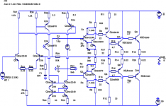
Coming back to the original thread, here's another (slightly more elaborated) power amp, loosely derived from MikeB's Symasym. I'll skip the FFT plots, and just summarize: At 45 V output amplitude (~125W into 8 ohms), it simulates with H2 ~= H3 at -80 dB from H1. That more or less reaches my original goal, so I'll take a break for a few days, take a few steps back and a few deep breaths, and then think about how to get to -100 dB at 100W. This has been a fairly intense and euphoric week.
I apologize - I realize that all kinds of insight, even incorrect ones, can improve one's understanding of reality.
I guess I went off the handle because of the suggestion that the original Kulish work was plagiarized - I haven't ever seen anything like it; however, I will readily concede that it may be superficially similar to earlier topologies developed around vacuum tubes or even BJTs. If such work exists, I would be interested in seeing the reference to it - papers, patents, schematics, anything...
Once again, my apologies to Hahfran.
Coming back to the original thread, here's another (slightly more elaborated) power amp, loosely derived from MikeB's Symasym. I'll skip the FFT plots, and just summarize: At 45 V output amplitude (~125W into 8 ohms), it simulates with H2 ~= H3 at -80 dB from H1. That more or less reaches my original goal, so I'll take a break for a few days, take a few steps back and a few deep breaths, and then think about how to get to -100 dB at 100W. This has been a fairly intense and euphoric week.
Attachments
Re: My sim is putting kulish in the lead !!
I stand corrected, yes, I can see that it is potentially superior to CFP
if it can be trimmed correctly.
http://www.diyaudio.com/forums/attachment.php?s=&postid=1388670&stamp=1199215345
From this circuit VBE error on Q2 creates the adjustment current
through R1 and manifests in R3.
The big thing here is that the 'adjustment' current generated
through R1 results in no voltage change in R4 and as such is
isolated.
However it appears to me that Kulish correction can only be used
as a voltage out arrangement and can not be used effectively in a
V-I converter such as a dif pair IP feeding a folded cascode VAS. The
ratio of load resistances are what allows it to work.
All this, in essence, is similar to the Hawksford dif pair correction
schemes, see fig 10 to fig 15 in this paper:
http://www.essex.ac.uk/dces/research/audio_lab/malcolmspubdocs/J4 Distortion correction circuits.pdf
Has anyone tried simulating, for example, fig 15 circuit?
cheers
Terry
DRC said:Hi,
I did another sim with a CFP diff stage for comparison (attached). Hopefully, this is the correct configuration for CFP- i set the current for the inner NPN to a similar value to the kulish configuration.
again 30V p-p output :
std diff THD
0.019198%
kulish THD
0.000306%
CFP diff
0.002518%
It is worth noting that the kulish version's THD is very sensitive to resistor value ...
/dave
x-pro said:
I would disagree. The circuits you've quoted are all feedback based where "Kulish Cell" is a true feedforward compensation approach, where adding two distorted currents results in an almost undistorted output. As a result it is much faster and it is also a very linear voltage to current convertor, useful in many applications.
In short - it is a different approach and could be a good alternative to more common NFB-based circuits.
Cheers
Alex
I stand corrected, yes, I can see that it is potentially superior to CFP
if it can be trimmed correctly.
http://www.diyaudio.com/forums/attachment.php?s=&postid=1388670&stamp=1199215345
From this circuit VBE error on Q2 creates the adjustment current
through R1 and manifests in R3.
The big thing here is that the 'adjustment' current generated
through R1 results in no voltage change in R4 and as such is
isolated.
However it appears to me that Kulish correction can only be used
as a voltage out arrangement and can not be used effectively in a
V-I converter such as a dif pair IP feeding a folded cascode VAS. The
ratio of load resistances are what allows it to work.
All this, in essence, is similar to the Hawksford dif pair correction
schemes, see fig 10 to fig 15 in this paper:
http://www.essex.ac.uk/dces/research/audio_lab/malcolmspubdocs/J4 Distortion correction circuits.pdf
Has anyone tried simulating, for example, fig 15 circuit?
cheers
Terry
> it appears to me that Kulish correction can only be used
as a voltage out arrangement and can not be used effectively in a
V-I converter such as a dif pair IP feeding a folded cascode VAS. The
ratio of load resistances are what allows it to work.
It can and does work as a very linear V-I converter - that's what I've used in the power stages which I simulated and described in this thread. The load resistance ratios are critical for ultra-low distortion (<-120 dB H2), but you can still get very good performance (say <-80 dB) with fairly loosely calculated resistor ratios.
Moreover, adding an additional load resistance from the corrected collector to ground does not alter the distortion picture greatly, only the gain (an unusual oddity is that smaller load resistors to ground actually result in lower distortion, as long as neither transistor gets biased to cutoff or saturation as a result). It's a pure transconductance amplifier, like a FET at constant Vds.
It also works as an LTP feeding a folded cascode, but there are tradeoffs (lower voltage gain) in such a topology, and biasing the cascode is a bit messy. Check out DRC's LTP simulations to see the linearity advantage with the Kulish LTP.
linuxguru,
I don't see any folded cascodes in the linked circuits or how you can use this cell in V-I without some way of scaling the two currents prior to mixing without considerable extra circuity.
I guess a pair of 'ratio' current mirrors could make a V-I from it (eg 1:R1 and 1:R1+R2 )
Did i miss something
Terry, I don't think i'll be able to resist sim-ing the fig15 feedforward diff from the hawksford paper
/dave
> I don't see any folded cascodes in the linked circuits
The only folded cascode in the circuits I posted used a stock LTP, not a Kulish.
A Kulish LTP is tricky to use with a folded cascode - but it's mainly a biasing
difficulty, not a topological impossibility.
> or how you can use this cell in V-I without some way of scaling the two currents prior to mixing without considerable extra circuity.
In the power stages I posted , the aim is to obtain *unity* voltage gain
at the load with the 3 stages. The Kulish pre-driver is a V-I (transconductance)
stage, and the remaining one or two stages are pure current-gain stages.
The exact current scaling turns out to be unimportant, because the 3
stages (pre-driver, driver and power output) are themselves wrapped
by an intermediate unity-gain voltage-series feedback loop that uses the
load impedance to develop the feedback voltage to the Kulish pre-driver.
The output stage will only deliver as much current as is required to
maintain the voltage across the load almost the same as the input
voltage at the base of the pre-driver, minus the bias offset of the Vbe
servo (say 1.2v or 1.5v).
Hence, the exact current gain of the three stages (pre-driver, driver and
power output) is not that important - it mostly affects the impedance
presented by the base(s) of the pre-driver to the VAS. That turns out to
be high enough (>1M) for typical values of load impedance (8 ohms)
and hfe of the driver and output transistors.
The only other issue is stability - if the intermediate loop gain is high enough,
there is every possibility of the output stage oscillating, especially with a
reactive load. This is more acute with the CFP output than the EF. However,
this problem is not due to the Kulish pre-driver, but a problem with any
output stage with a similar topolgy, including classic CFP and EF output
stages, and can be dealt with in the usual ways - Zobel network, series
inductance, lag compensation, external collector-base capacitances on
the CFP devices, etc.

- Status
- This old topic is closed. If you want to reopen this topic, contact a moderator using the "Report Post" button.
- Home
- Amplifiers
- Solid State
- Kulish Corrector for Class-A EF O/P Stage